Light emitting device and manufacturing method thereof

a technology of light emitting devices and manufacturing methods, applied in the direction of discharge tubes/lamp details, discharge tubes luminescnet screens, organic semiconductor devices, etc., can solve the problems of poor electric current injection efficiency, low efficiency of conductive oxide films, and slow response of elements, so as to increase the breadth of selectable materials capable of being used as anodes, the effect of high electric current injection efficiency and superior responsibility

Inactive Publication Date: 2005-04-19
SEMICON ENERGY LAB CO LTD
View PDF20 Cites 86 Cited by
  • Summary
  • Abstract
  • Description
  • Claims
  • Application Information

AI Technical Summary

Benefits of technology

[0014]The breadth of selectable materials capable of being used as an anode is increased by thus implementing the present invention, and it becomes possible to obtain a light emitting device having a driver voltage which is lower, and having an emitted light luminance which is higher, compared to a conventional light emitting device. Furthermore, it becomes possible to use metallic films and semiconductor films, whose resistance is lower than that of conductive oxide films, as an anode, and therefore a light emitting device having high electric current injection efficiency and having superior responsibility can be obtained.

Problems solved by technology

Conductive oxide films transmit visible light, and therefore light emitted from an EL layer can be easily extracted, but conductive oxide films have the disadvantage of high resistance compared to metallic films.
Not only does the injection efficiency of electric current into an EL layer become poor when the anode resistance is high, but a problem of an element having slow response arises.
Conductive oxide films are formed by evaporation or sputtering, and there are many problems such as dust or other refuse during film formation.
Furthermore, there is a problem in that etching becomes difficult due to crystallization, and therefore, conductive oxide films are one of the kinds of conductive films which are difficult to handle when compared to metallic films.
However, EL light emitting device cathodes are metallic films, and therefore there is a problem in that emitted light cannot be extracted if a transparent conductive film is not used in the anode.

Method used


Image

  • Light emitting device and manufacturing method thereof
  • Light emitting device and manufacturing method thereof
  • Light emitting device and manufacturing method thereof

Examples


embodiment 1

[Embodiment 1]

[0068]A light emitting device having a pixel portion with a structure differing from that of FIGS. 1A to 3B is explained in Embodiment 1. FIGS. 5A to 5C, and FIG. 6 are used in the explanation.

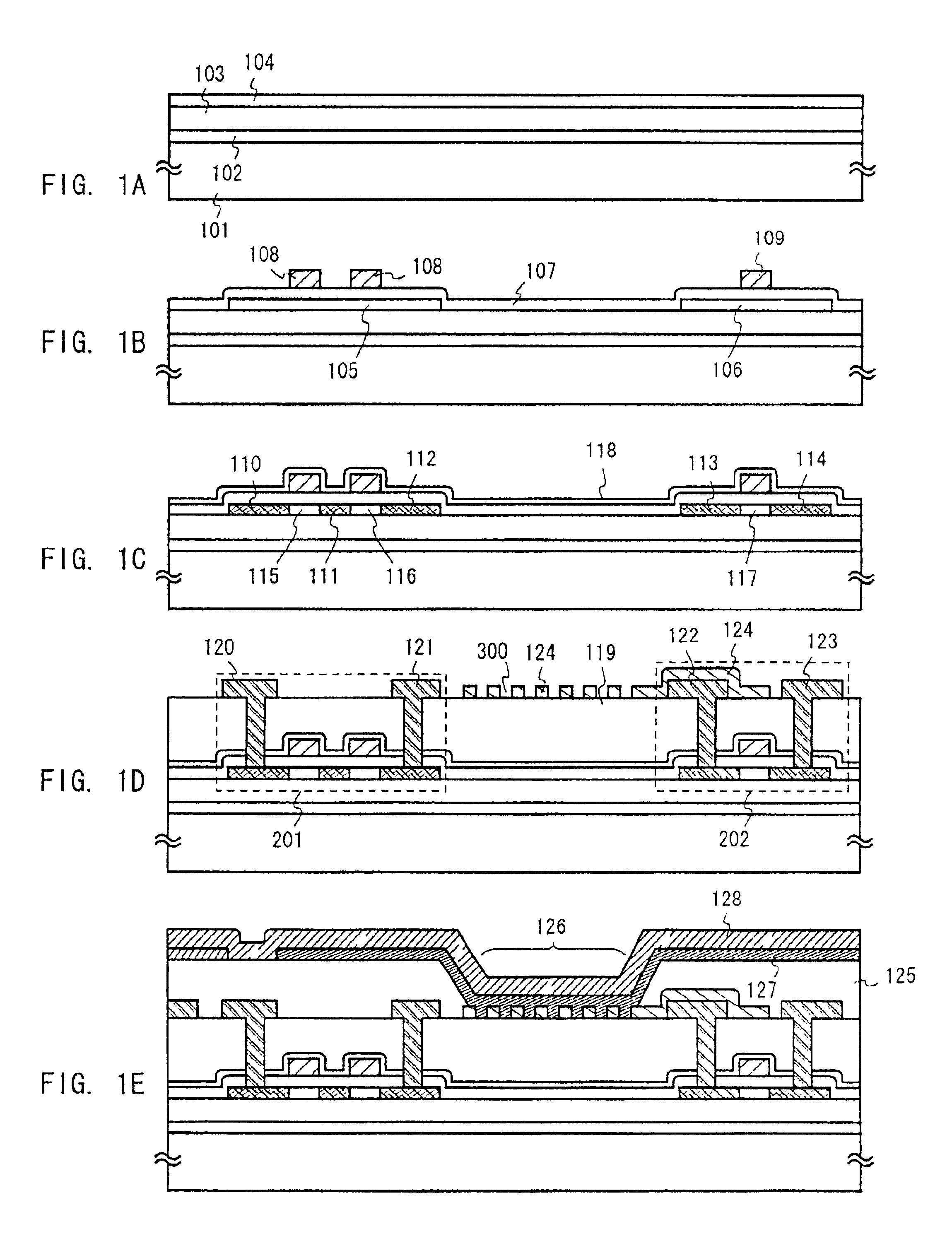
[0069]Processing is first performed in accordance with the manufacturing steps of FIG. 1 up through FIG. 1D. However, a slit is not formed in a pixel electrode 501 in Embodiment 1. Further, platinum is used as a material for forming the pixel electrode 501 in Embodiment 1. (See FIG. 5A.)

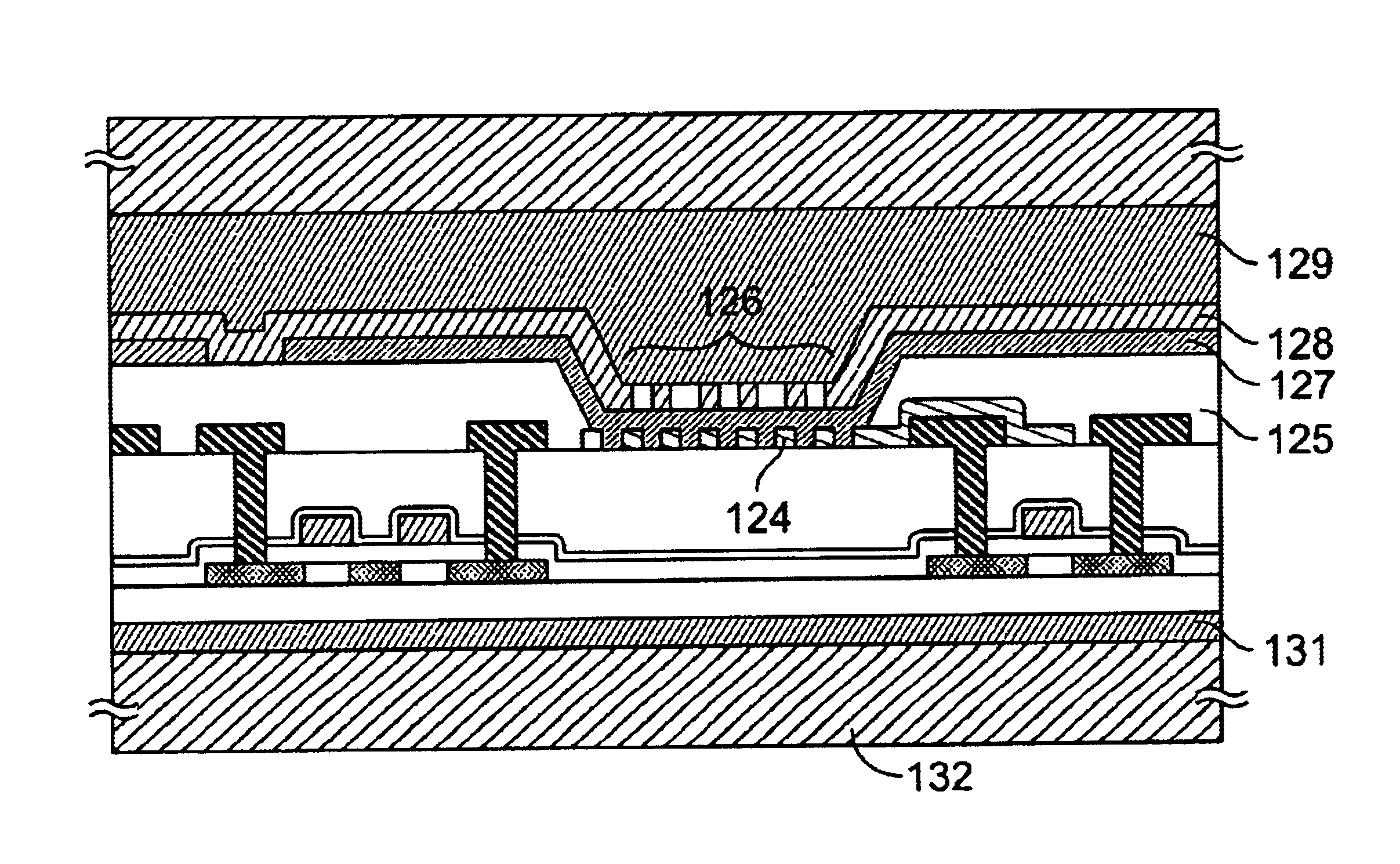
[0070]The second interlayer insulating film 125 is formed next, as explained in the embodiment mode of the present invention, and the opening portion 126 is formed, and an organic EL layer 502 is formed. The EL layer 502 may be formed in accordance with the embodiment mode. Further, a cathode 503 is formed on the EL layer 502. An aluminum film to which lithium has been added is used as the cathode 503 in Embodiment 1. Note that evaporation is used for the film formation of the cathode 503, and tha...

embodiment 2

[Embodiment 2]

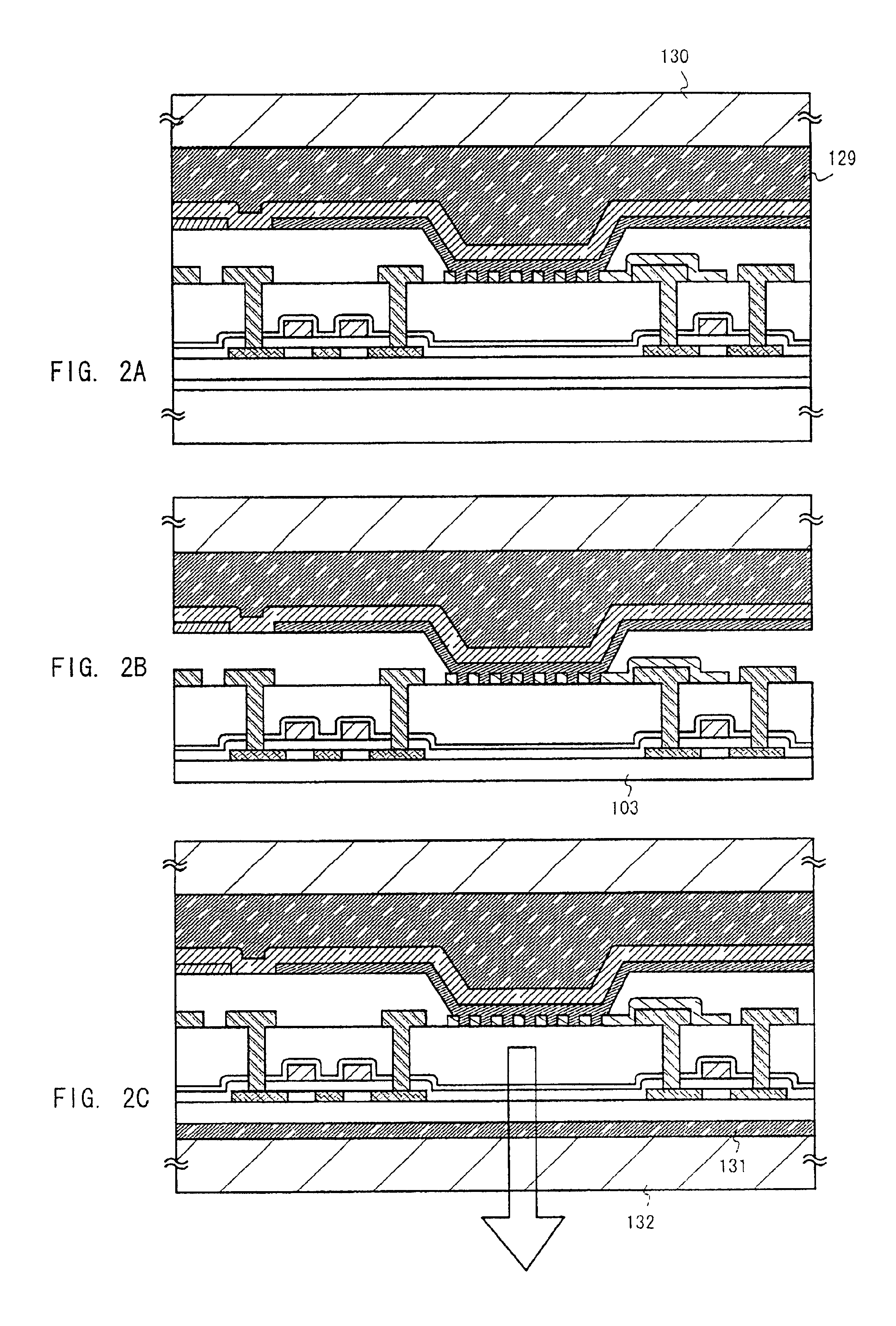
[0075]In Embodiment 2, formation of a DLC (diamond-like carbon) film in one or both surfaces of the fixing substrate and / or the joining substrate is effective. However, the transitivity drops if the film thickness is too thick, and therefore the film thickness may be set equal to or less than 50 nm (preferably between 10 and 20 nm).

[0076]The DLC film has a Raman spectral distribution with an asymmetric peak at approximately 1550 cm−1, and a shoulder at approximately 1300 cm−1. Further, it shows a hardness of 15 to 25 Pa when measured using a microhardness meter.

[0077]The DLC film has a larger hardness compared to a plastic substrate, and has a larger thermal conductivity, and is therefore effective when formed as a protecting film for surface protection and thermal diffusion.

[0078]It is therefore possible to form the DLC film in advance before joining the plastic substrate, or to form the DLC film after joining the plastic substrate. Whichever structure is used, the DL...

embodiment 3

[Embodiment 3]

[0079]An EL light emitting device of the present invention can be given with a pixel portion having the circuit configuration shown in FIG. 7. In FIG. 7, reference numeral 701 denotes a source wiring, reference numeral 702 denotes a gate wiring, 703 denotes a switching TFT, 704 denotes a current control TFT, 705 denotes a current supply line, and reference numeral 706 denotes an EL element. The switching TFT 703 and the current control TFT 704 are manufactured by p-channel TFTs in Embodiment 3. One of the switching TFT 703 and the current control TFT 704 may be an n-channel TFT, of course, and both may also be n-channel TFTs.

[0080]Note that the same role as the capacitor 301 of FIGS. 3A and 3B is supplemented by a gate capacitor of the current control TFT 704. This is because one frame period (or one field period) is short when performing time-division gray-scale display in accordance with digital drive so that an electric charge can be maintained by only the gate capa...


PUM


Abstract

A light emitting device having superior responsibility is provided. A pixel electrode (anode) connected to a drain wiring of an current control TFT has a slit. The slit becomes a path for light emitted from an EL layer, and emitted light can be extracted using a light shielding metallic film as the pixel electrode. A material having a low resistance can thus be used as the pixel electrode, and therefore a light emitting device having superior responsibility can be obtained.

Description

BACKGROUND OF THE INVENTION[0001]1. Field of the Invention[0002]The present invention relates to a device having an element in which a light emitting material is sandwiched between electrodes (hereafter referred to as a light emitting element), and to a method of manufacturing thereof. In particular, the present invention relates to a light emitting device using a light emitting element which utilizes a light emitting material in which EL (electro luminescence) is obtained as the light emitting material (hereafter referred to as an EL light emitting device, an EL element, and an EL material, respectively).[0003]Note that EL materials which can be used in the present invention include all light emitting materials in which light is emitted via singlet state excitation, triplet state excitation, or both types of excitation (phosphorescence and / or fluorescence).[0004]2. Description of the Related Art[0005]Development of EL light emitting devices has advanced in recent years. An EL light...

Claims


Application Information

Patent Timeline
Patent Type & Authority Patents(United States)
IPC IPC(8): H01L27/32H01L51/52H01L27/28H01L51/50
CPCH01L51/5203H01L51/5234H01L51/5206H01L27/3244H01L2251/5315H10K59/12H10K50/813H10K50/828H10K2102/3026H10K59/805H10K50/805
Inventor YAMAZAKI, SHUNPEI
Owner SEMICON ENERGY LAB CO LTD
Why Eureka
Try Eureka