Vertical MOSFET reduced in cell size and method of producing the same

a technology of semiconductor field effect transistor and vertical mosfet, which is applied in the direction of semiconductor devices, electrical equipment, basic electric elements, etc., can solve the problems of reducing the vt or source resistance of the photolithography process, requiring two masking steps, and disadvantages, etc., to achieve the effect of reducing the cell size without increasing the vt or the source resistan

Inactive Publication Date: 2005-05-03
RENESAS ELECTRONICS CORP
View PDF7 Cites 63 Cited by
  • Summary
  • Abstract
  • Description
  • Claims
  • Application Information

AI Technical Summary

Benefits of technology

[0014]It is an object of this invention to provide a vertical MOSFET reduced in cell size without increasing Vt or a source resistance in case where a trench contact structure with a trench formed in each of a source layer and a base layer is used in a UMOSFET as the vertical MOSFET.

Problems solved by technology

Therefore, a photolithography process requiring two masking steps is unnecessary.
It is also possible to narrow the contact width by filling W. On the other hand, the above-mentioned structure is disadvantageous in the following respects.
It is therefore difficult to form the oxide film by LOCOS or to control the thickness of the oxide film, Generally, bird's beak in LOCOS has a length substantially equivalent to the thickness.
However, the above-mentioned structure is disadvantageous in the following respects.
In addition, in case of typical Al sputtering at a temperature of 100 to 300° C., the coverage is inferior.
If a contact hole is small, a void is produced and the contact hole can not sufficiently be filled.
Even if the contact hole is filled, a surface profile becomes irregular when the Al coverage is inferior.
Furthermore, there is another disadvantage in common to both of the structures.
As a consequence, miniaturization of the cell can not be achieved.

Method used


Image

  • Vertical MOSFET reduced in cell size and method of producing the same
  • Vertical MOSFET reduced in cell size and method of producing the same
  • Vertical MOSFET reduced in cell size and method of producing the same

Examples


Embodiment Construction

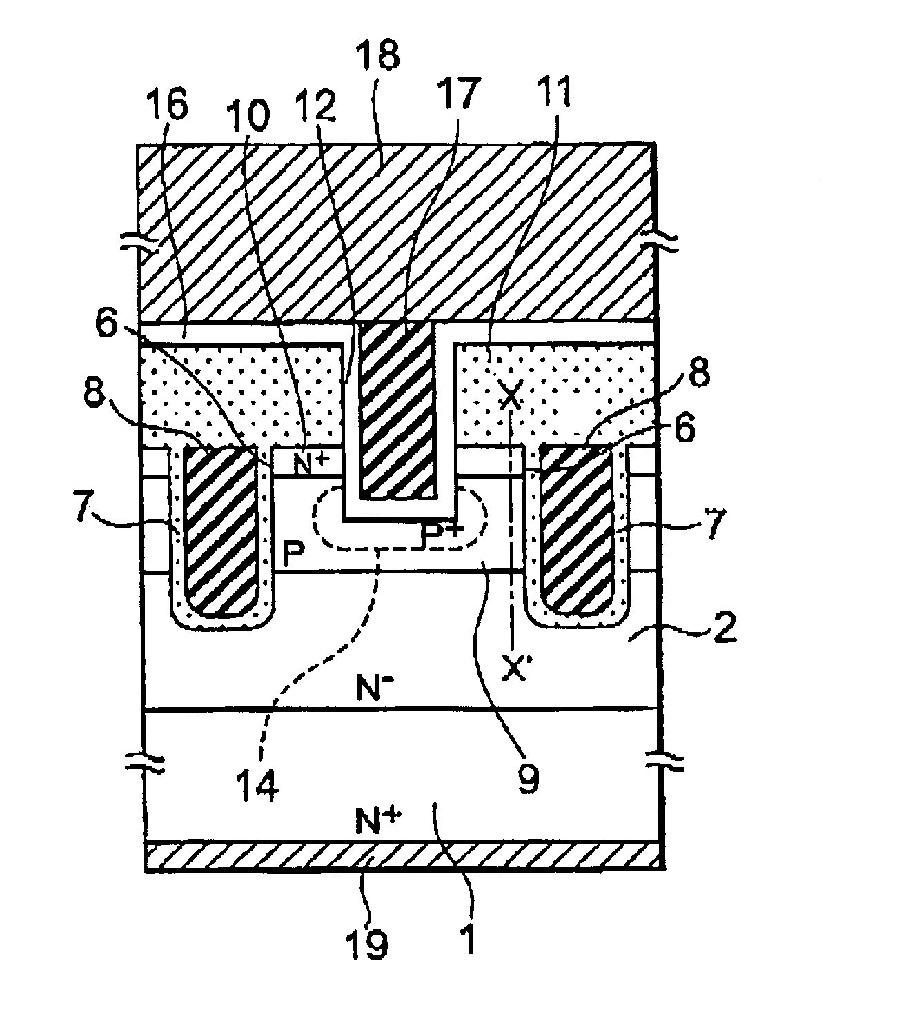
[0049]Now, description will be made of an embodiment of this invention with reference to the drawing.

[0050]Referring to FIGS. 3A, 3B, 4A, and 4B, a UMOSFET chip may have various layouts of cells. In FIG. 3A, a plurality of square cells are arranged in a matrix. In FIG. 3B, the square cells are arranged in a matrix and the cells in adjacent lines are offset in position from each other. In FIG. 4A, a plurality of hexagonal cells are arranged. In FIG. 4B, a plurality of elongated cells are arranged in a column direction. As a matter of convenience, unit cells 101, 201, and 301 in each figure can be defined as structural units separated by trenches 106, 206, and 306 where gate electrodes are to be formed. At the centers of the unit cells 101, 201, and 301, contact holes 112, 212, and 312 are disposed, respectively. The contact holes may have any desired shape, such as a square shape, a hexagonal shape, an octagonal shape, and a circular shape. If the contact hole is sufficiently small, ...


PUM


Abstract

In a vertical MOSFET comprises: a semiconductor layer (1, 2, 9, 10) having first and second surfaces opposite to each other and trenches (6) formed on the first surface; trench gates (8) formed in the trenches; a unit cell formed in a region of the semiconductor layer surrounded by the trench gates, the unit cell comprising a base layer (9) and a source layer (10) formed on the base layer and having the first surface as a principal semiconductor surface, the unit cell having a contact hole (12) formed on a center of the principal semiconductor surface and extending from the principal semiconductor surface through the source layer to an inside of the base layer; a contact (17) formed in the contact hole; a source electrode (18) formed on the contact; and a drain electrode (19) formed on the second surface, the contact is formed to a depth different to a peak depth which is a position having a maximum impurity-concentration in a depth direction of the base layer. The unit call further comprises a base contact layer (14) formed within the base layer so as to enclose a bottom of the contact and to bring the base contact layer into contact with the bottom of the contact.

Description

BACKGROUND OF THE INVENTION[0001]This invention relates to a vertical MOSFET (Metal Oxide Semiconductor Field Effect Transistor) reduced in cell size and, in particular, to a MOSFET (UMOSFET) with a gate electrode formed in a U-shaped trench and a method of producing the same.[0002]An orthogonal field effect transistor (MOSFET) is a device used in the field of power electronics. Depending upon an apparatus to which the vertical MOSFET is applied, a breakdown voltage (drain-source breakdown voltage: BVdss) between several tens to several hundreds of volts (V) is required. In addition, there is technical trend towards low power consumption by reducing an on-resistance (Ron) during an on-period (during operation), high-speed operation by reducing a parasitic capacitance and a parasitic resistance, improvement of breakdown resistance in a severe operation environment, and improvement of trade-off among these characteristics.[0003]In order to reduce the on-resistance while maintaining a ...

Claims


Application Information

Patent Timeline
Patent Type & Authority Patents(United States)
IPC IPC(8): H01L21/02H01L29/66H01L21/336H01L29/78H01L21/265H01L29/45H01L29/40H01L21/28H01L29/417H01L29/423H01L29/49
CPCH01L29/7813H01L21/26586H01L29/41766H01L29/7802H01L29/456
Inventor KOBAYASHI, KENYA
Owner RENESAS ELECTRONICS CORP
Why Eureka
Try Eureka