

Alignment or overlay marks for semiconductor processing
a technology of alignment or overlay marks and semiconductors, applied in the direction of semiconductor devices, semiconductor/solid-state device details, electrical apparatus, etc., can solve the problems of poor signal-to-noise ratio of alignment marks, adversely affecting overlay measurement capabilities, and exacerbated problems, so as to increase the signal-to-noise ratio
- Summary
- Abstract
- Description
- Claims
- Application Information
AI Technical Summary
Benefits of technology
Problems solved by technology
Method used
Image

Examples
Embodiment Construction
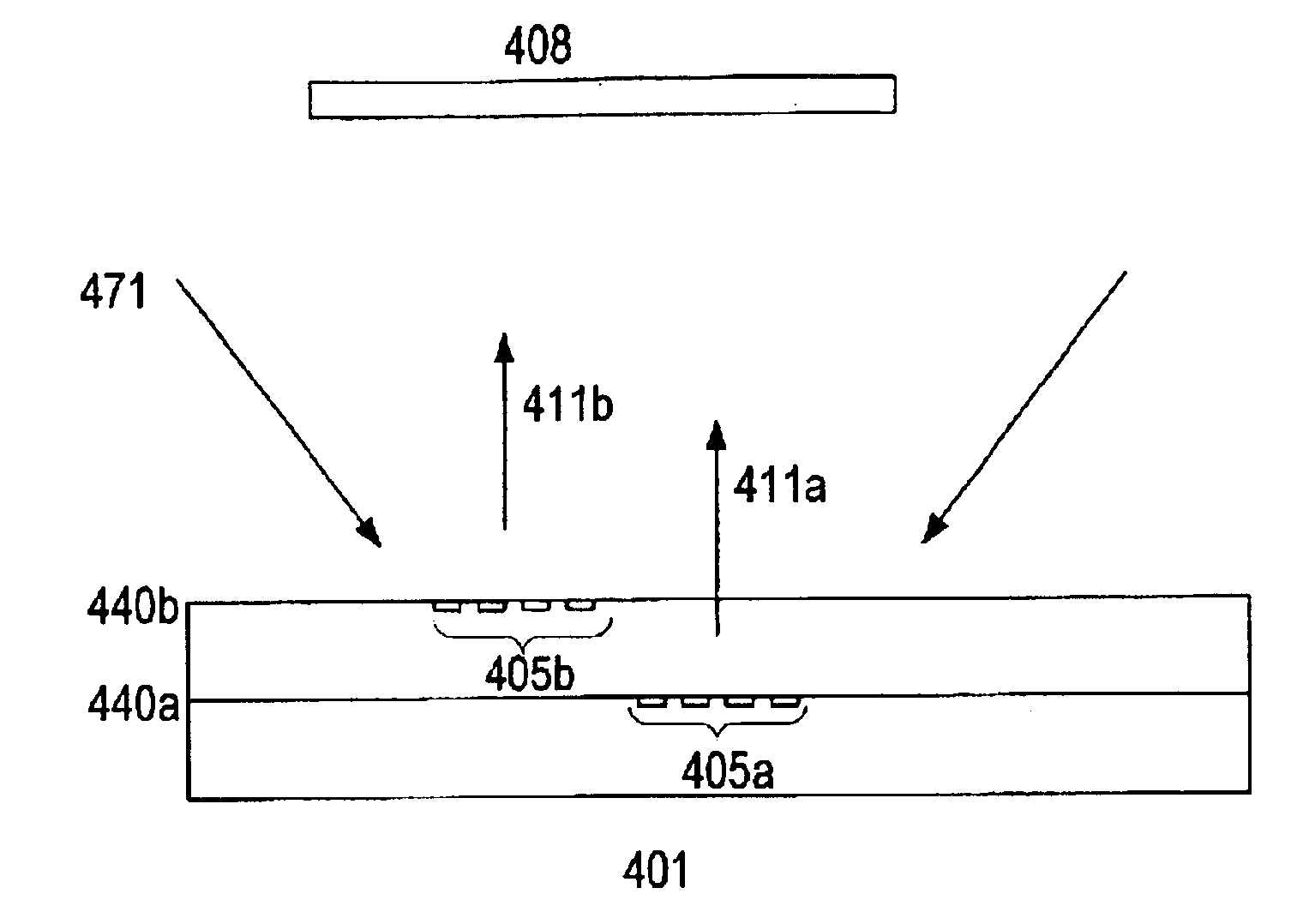
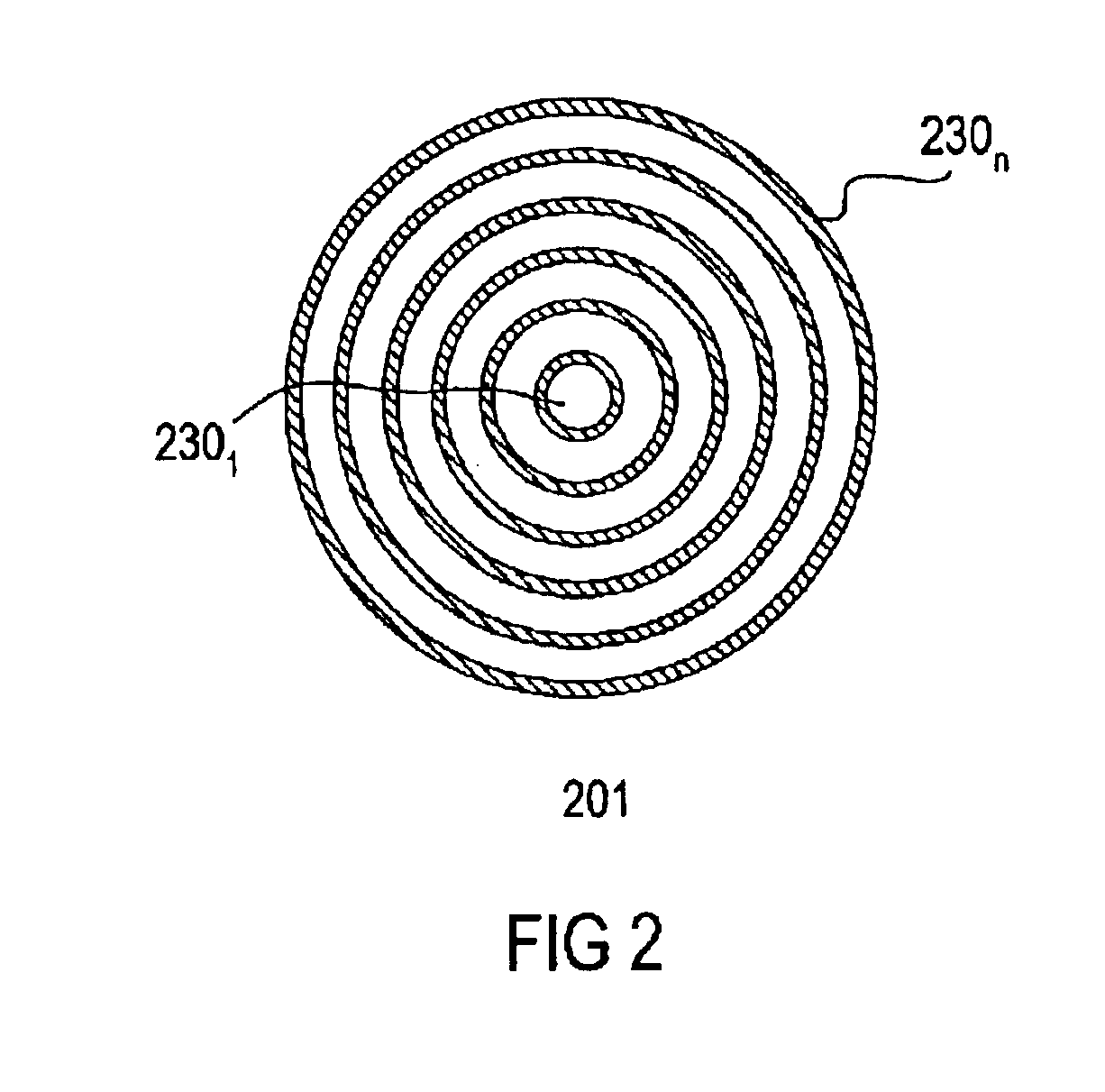
[0013]The invention relates generally to the fabrication of ICs such as memory ICs. Other types of ICs are also useful. Generally, a plurality of ICs are formed on a semiconductor substrate, such as a silicon wafer, in parallel. After processing is finished, the wafer is diced to separate the ICs into individual chips. The chips are then packaged, resulting in a final product that is used in, for example, consumer products such as computer systems, cellular phones, personal digital assistants (PDAs), and other electronic products. In particular, the invention relates to alignment marks used in semiconductor processing.
[0014]FIG. 2 shows an alignment mark in accordance with one embodiment of the invention. As shown, the alignment mark comprises at least one geometric zone plate 201. Zone plates are described in, for example, Guillermo Penate, “Zone Plate: a quasi scientific explanation” (1999), which is herein incorporated by reference for all purposes. Preferably, the alignment mark...
PUM
 Abstract
Description
Claims
Application Information