Test head assembly for electronic components with plurality of contoured microelectronic spring contacts

Inactive Publication Date: 2005-05-03
FORMFACTOR INC
View PDF74 Cites 142 Cited by
  • Summary
  • Abstract
  • Description
  • Claims
  • Application Information

AI Technical Summary

Benefits of technology

[0014]Semiconductor devices with contacts according to the present invention may be either socketed to a mating electronic component, or soldered. Underfill is not required and typically is not preferred. Instead, an unfilled gap between the device and the mating component allows for relative movement between the device and the mated component to accommodate differences in thermal expansion and contraction, and allows for venting of any trapped moisture or other unwanted volatile materials. An unfilled gap may also be advantageous for cooling the device, by providing an additional channel for forced convective cooling. A stop structure, if present between the device and the mated component, is preferably detached from at least one of the device or the mated component, and therefore permits relative movement to accommodate thermal expansion and contraction. When devices provided with contacts according to the invention are soldered to a mated component, solder need only be present on the distal end of each spring contact, thereby distancing it from the semiconductor device and greatly reducing the soft error rate caused by solder-generated Alpha particles.
[0015]In an alternative embodiment, an LGA socket is provided with molded

Problems solved by technology

As semiconductor devices are made in increasingly smaller sizes, while at the same time becoming increasingly complex, semiconductor die size, and the size of contacts pads on such dice, has also shrunk.
A soldered joint between such mismatched materials is subject to stresses from thermal cycling, which over time can weaken the joint and degrade the electrical performance of the soldered CSP/PCB system.
Traditional approaches, such as underfilling, can reduce problems caused by mismatched thermal properties, but such approaches are difficult to scale down to increasingly smaller sizes.
In additi

Method used


Image

  • Test head assembly for electronic components with plurality of contoured microelectronic spring contacts
  • Test head assembly for electronic components with plurality of contoured microelectronic spring contacts
  • Test head assembly for electronic components with plurality of contoured microelectronic spring contacts

Examples


Embodiment Construction

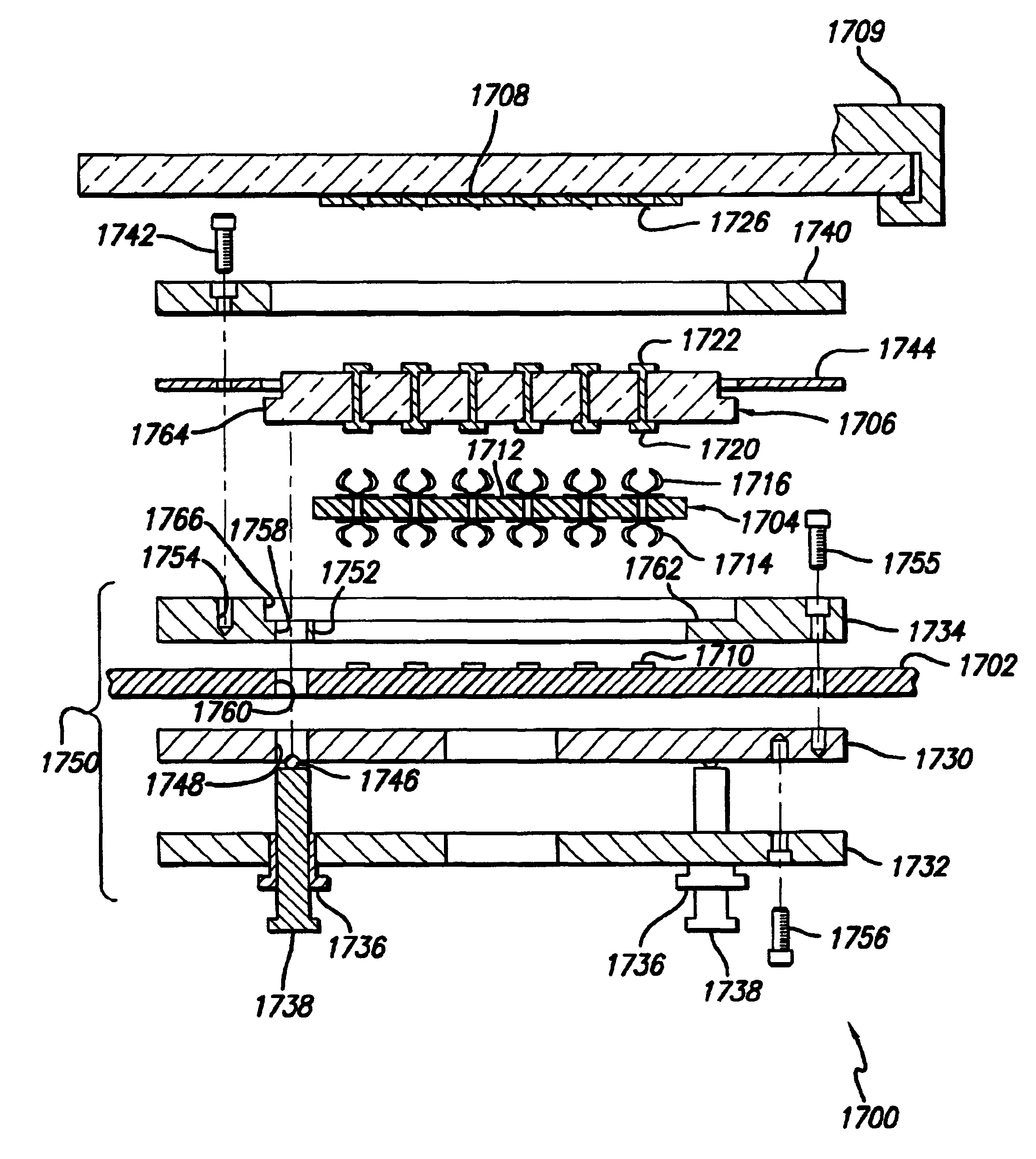
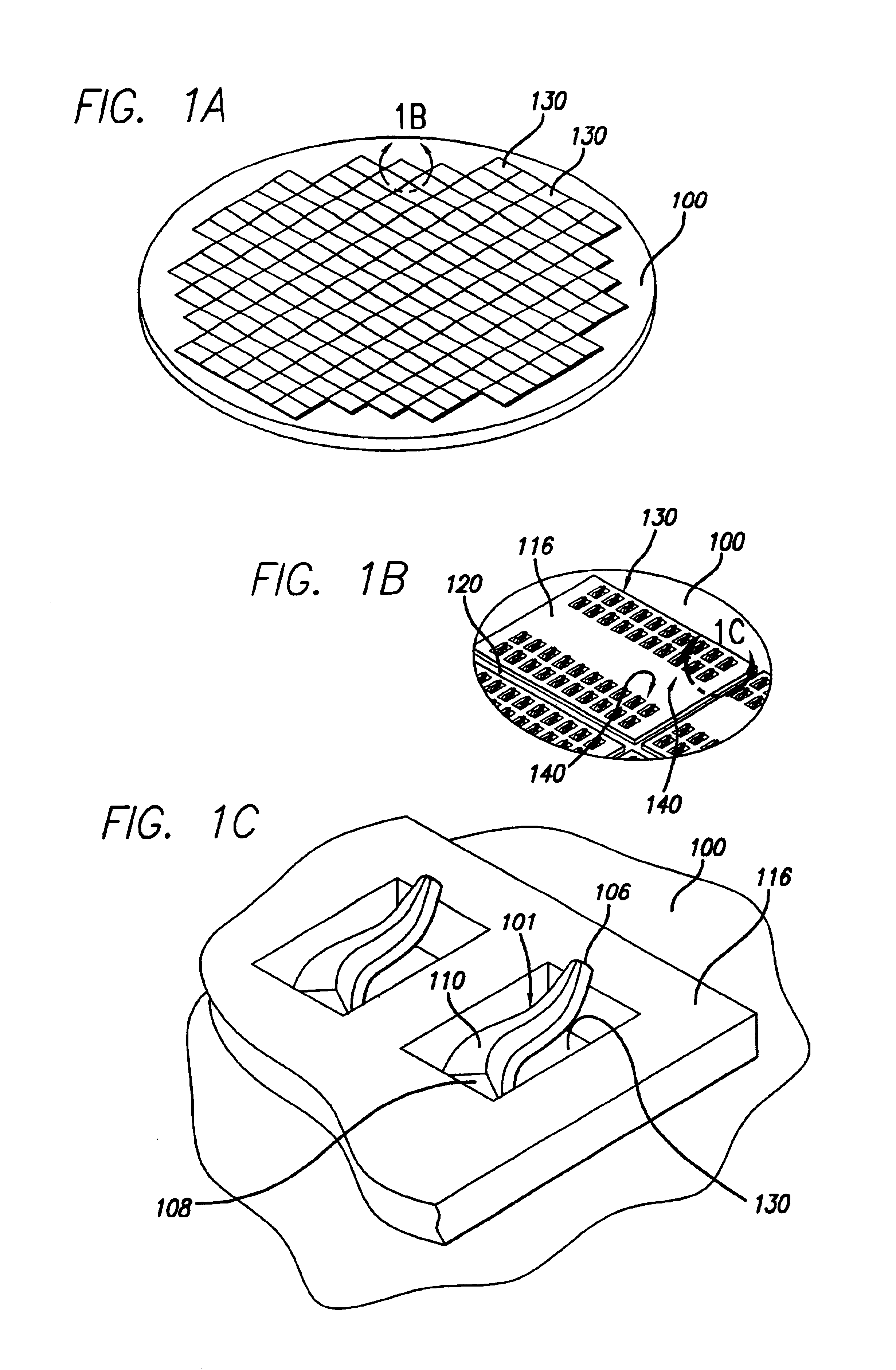
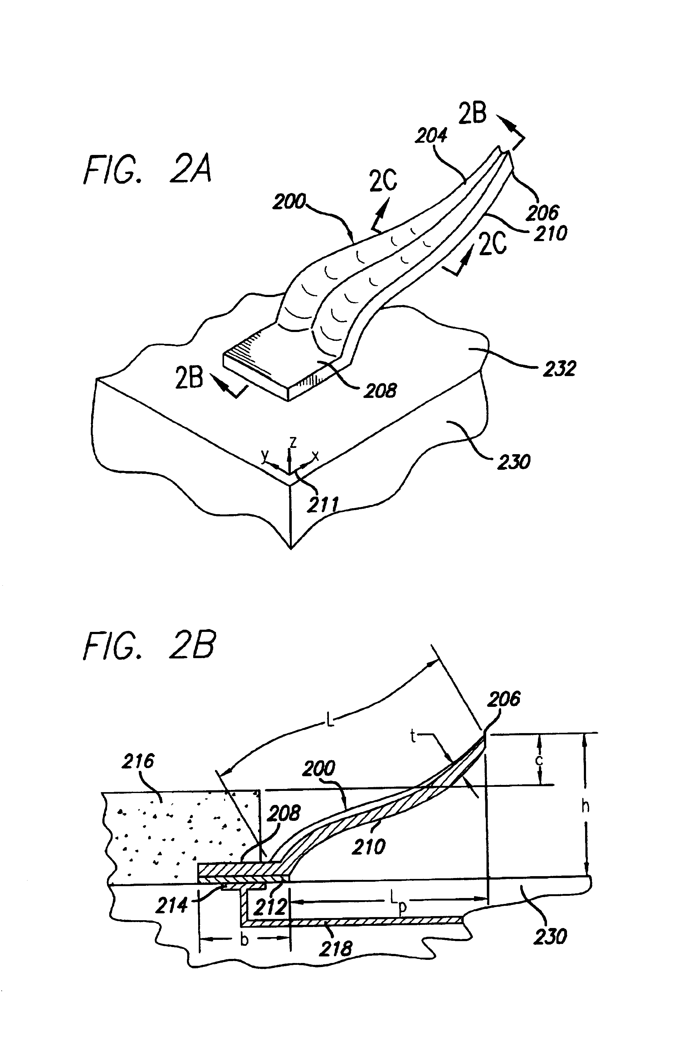
[0050]The present invention satisfies the need for an electronic component with a plurality of microelectronic spring contacts, that overcomes the limitations of prior art components provided with interconnection elements. In the detailed description that follows, like element numerals are used to describe like elements illustrated in one or more figures.

[0051]Contoured spring contacts according to the present invention are particularly well-suited to making electrical connections to microelectronic devices having contact pads disposed at a fine-pitch, or where a large array of economical microelectronic spring contacts is desired. “Fine-pitch” refers to microelectronic devices that have their contact pads disposed at a spacing of less than about 130 microns (5 mils), such as 65 microns (2.5 mils). However, structures of the present invention may also be used in coarser-pitch applications, if desired. The advantages of the present invention are realized in part from the close tolera...


PUM


Abstract

An electronic component is disclosed, having a plurality of microelectronic spring contacts mounted to a planar face of the component. Each of the microelectronic spring contacts has a contoured beam, which may be formed of an integral layer of resilient material deposited over a contoured sacrificial substrate, and comprises a base mounted to the planar face of the component, a beam connected to the base at a first end of the beam, and a tip positioned at a free end of the beam opposite to the base. The beam has an unsupported span between its free end and its base. The microelectronic spring contacts are advantageously formed by depositing a resilient material over a molded, sacrificial substrate. The spring contacts may be provided with various innovative contoured shapes. In various embodiments of the invention, the electronic component comprises a semiconductor die, a semiconductor wafer, a LGA socket, an interposer, or a test head assembly.

Description

RELATED APPLICATION[0001]This application is a continuation-in-part of the U.S. patent application, filed Feb. 27, 2001, now U.S. Pat. No. 6,780,001 entitled “FORMING TOOL FOR FORMING A CONTOURED MICROELECTRONIC SPRING MOLD,” by Eldridge and Wenzel (Ser. No. 09 / 795,772), which is a continuation-in-part of co-pending U.S. patent application, filed Feb. 12, 2001, entitled “METHOD FOR FORMING MICROELECTRONIC SPRING STRUCTURES ON A SUBSTRATE,” by Eldridge and Wenzel (Ser. No. 09 / 781,833), which is a continuation-in-part of co-pending U.S. patent application Ser. No. 09 / 710,539, filed Nov. 9, 2000, entitled “LITHOGRAPHIC SCALE MICROELECTRONIC SPRING STRUCTURES WITH IMPROVED CONTOURS,” by Eldridge and Wenzel, which applications are incorporated herein, in their entirety, by reference, and which are collectively referred to herein as the “parent applications.”BACKGROUND OF THE INVENTION[0002]1. Field of the Invention[0003]The present invention relates to electronic component substrates wit...

Claims


Application Information

Patent Timeline
IPC IPC(8): G01R1/067H01L23/48H05K7/10G01R1/04G01R1/02G01R1/073H01R13/24H01R13/22H05K3/40H01R12/61G01R3/00
CPCG01R1/0483G01R1/06727G01R1/06716G01R1/07342H01L24/72H01R13/2407H01R13/2442H05K7/1069H01R12/52G01R1/06711G01R1/06733G01R1/06744G01R1/06761G01R3/00H01L2924/01005H01L2924/01013H01L2924/01015H01L2924/01027H01L2924/01029H01L2924/01039H01L2924/01042H01L2924/01046H01L2924/01049H01L2924/01074H01L2924/01078H01L2924/01079H01L2924/01082H01L2924/04953H01L2924/14H01L2924/30107H01R2201/20H05K3/4092H01R12/714H01L2924/01006H01L2924/01023H01L2924/01033H01L2924/01047H01L2924/01087H01L2924/15787H01L2924/12042H01L2924/00
Inventor ELDRIDGE, BENJAMIN N.WENZEL, STUART W.
Owner FORMFACTOR INC
Why Eureka
Try Eureka