
High speed serial interface

a serial interface and high-speed technology, applied in the direction of synchronising signal speed/phase control, digital transmission, pulse technique, etc., can solve the problems of critical bottleneck in overall system performance, affecting the overall throughput of the system, and affecting the cost of increasing hardware requirements, so as to achieve accurate frequency and phase locking, high speed, and maximize throughput

Inactive Publication Date: 2005-05-17
MEDIATEK INC
View PDF2 Cites 34 Cited by
  • Summary
  • Abstract
  • Description
  • Claims
  • Application Information

AI Technical Summary

Benefits of technology

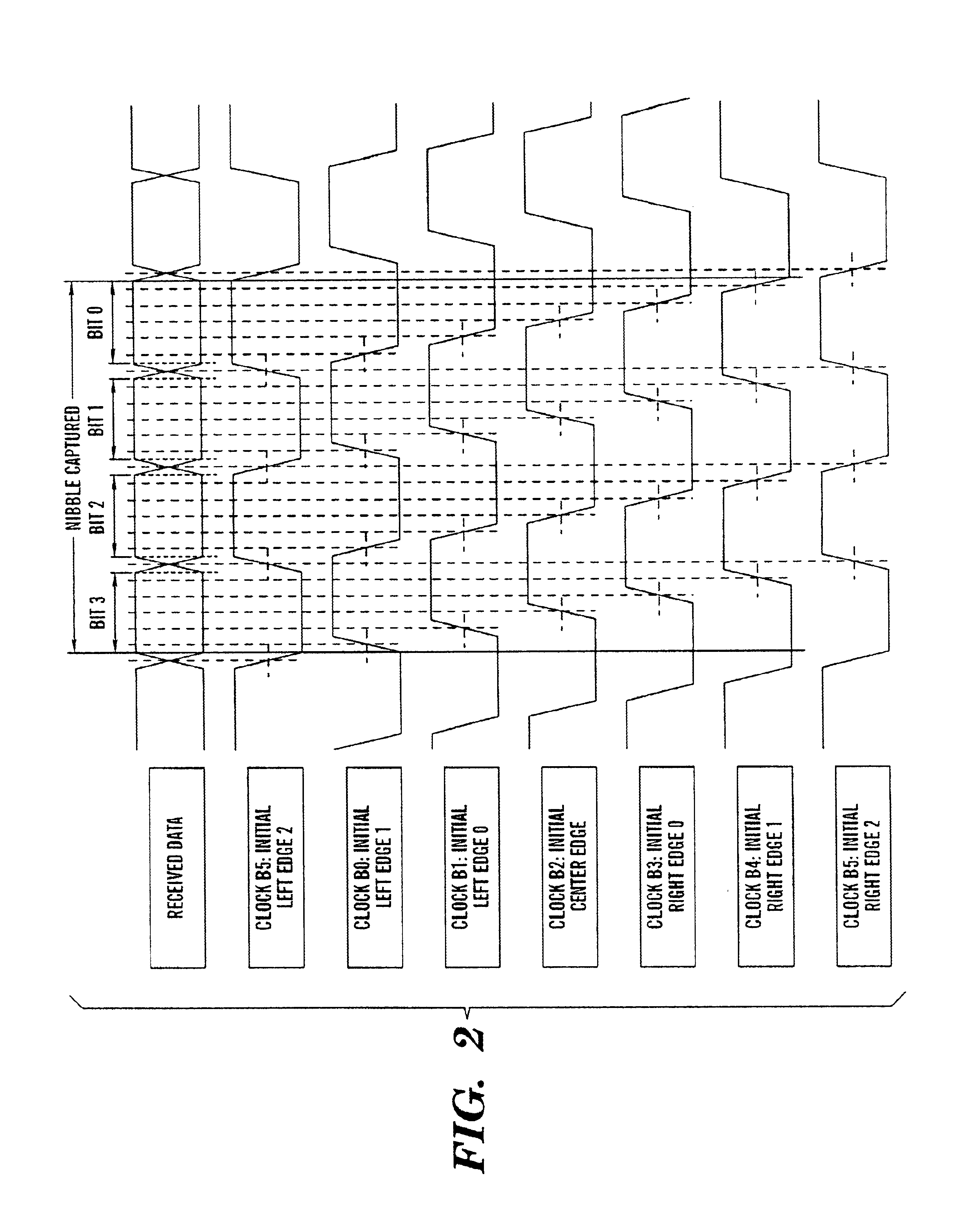
The present invention provides a high speed serial interface that solves problems of ASIC-to-ASIC high speed data transmissions by providing accurate frequency and phase locking between transmitted and received data. The interface allows data to be transmitted on each edge of a clock to maximize throughput and provides multiple parallel data paths to acquire data at discrete and predictable phase intervals. The interface also allows for compensation for transmitter to receiver phase delay drift over time and can filter out the effect of short term noise on an individual bit or bits. The interface can be used with multiple transmitter to receiver connections and can even compensate for different phase delays in each connection. The technical effects of the invention include improved data transmission accuracy, improved data transmission speed, and improved data transmission reliability.

Problems solved by technology

Often, this issue becomes the critical bottleneck in overall system performance.
This is readily apparent when considering communications systems where the overall throughput of the system (also referred to as the bandwidth of the system) is a fundamental limitation in determining how successfully the system can perform its intended application.
However, increasing the hardware requirements has a direct impact on cost in that the lower the overall bandwidth of a given IC package, the more IC packages become necessary to fulfill the total bandwidth requirement for this system.
Unfortunately, there is a limit on the available bandwidth of any given IC package I / O due to the fact that as data transfer rates (i.e. frequency) between IC's increase, the reliably of the transferred data decreases.
Reliability becomes particularly problematic in high speed transfers where a predictable phase relationship between the transmitted data, the received data, and the clocks on both the transmit and receive sides must be maintained in order to provide a synchronous timebase for the two discrete packages.
With older process technologies, it was fortunate that the package I / O bandwidth was typically greater than the computational bandwidth, i.e., the inherent bandwidth limitations imposed by the operating performance of the process technology.
Unfortunately, today's modem sub-micron process technologies provide internal ASIC (Application Specific Integrated Circuits) operating performance that results in computational bandwidths that far surpass the available package I / O bandwidths required in today's systems.
Techniques, such as transmitting data on both edges of the clock, push achievable bandwidths to 200 Mbs per package pin, but are still far from what is desired.
The problem with this solution is that the number of package I / O pins required to result in an I / O bandwidth that can provide adequate package to package bandwidth that will meet the requirements of the internal processing capabilities can lead to a very large pin count, and hence very expensive packages.
For the rare application, this may be acceptable, but for most applications this solution is prohibitively expensive.
At high bit rates (>300 Mbs), one of the major issues to contend with then becomes the overall time it takes to transmit data from one ASIC to another since this time can become a significant portion (if not greater than) the ideal duration (in time) of the data bit.
The problem with this solution is that tight phase coherence must be maintained over all of the LVDS I / O to LVDS I / O connections for the data and the clock.
Maintaining this phase coherence for a significant ratio of data connections to clock connections (e.g., >8) is extremely difficult for high bandwidth transmission (e.g., >500 Mbs per data bit=250 Mbs per package pin) since everything in this connection path must have exactly matched lengths.
The problem with this technique is that a unique PLL is required for every data input at the receiver ASIC.
This technique has the advantage of eliminating any phase coherency requirements between data inputs at the receiver (since each input is individually phase aligned), but has a couple of significant drawbacks that limit its usefulness.
A second problem is that the solution is inherently frequency dependent.
Once the design is implemented (i.e., fabricated), it cannot be guaranteed to operate at less than the lower limit of the frequency range it was designed for.
Yet a third problem is that this type of implementation has an inherent limitation in its ability to track for transmitter to receiver phase delay drift over time without significantly increasing the number of delay elements.
Therefore it can be seen that any appreciable amount of phase delay compensation would necessarily result in significantly more delay elements in the data delay chain.

Method used


Image

  • High speed serial interface
  • High speed serial interface
  • High speed serial interface

Examples


Embodiment Construction

I. Overview

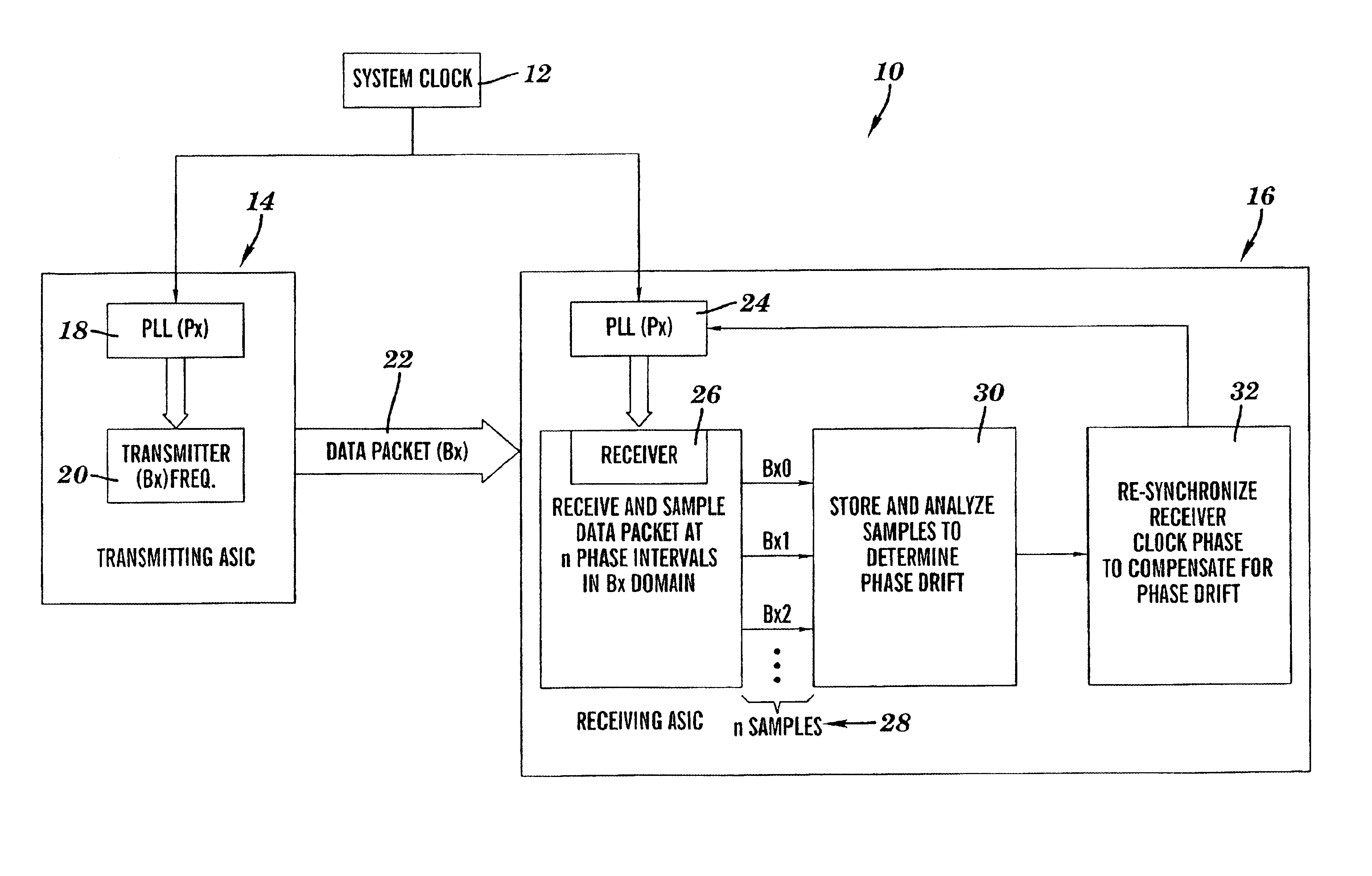
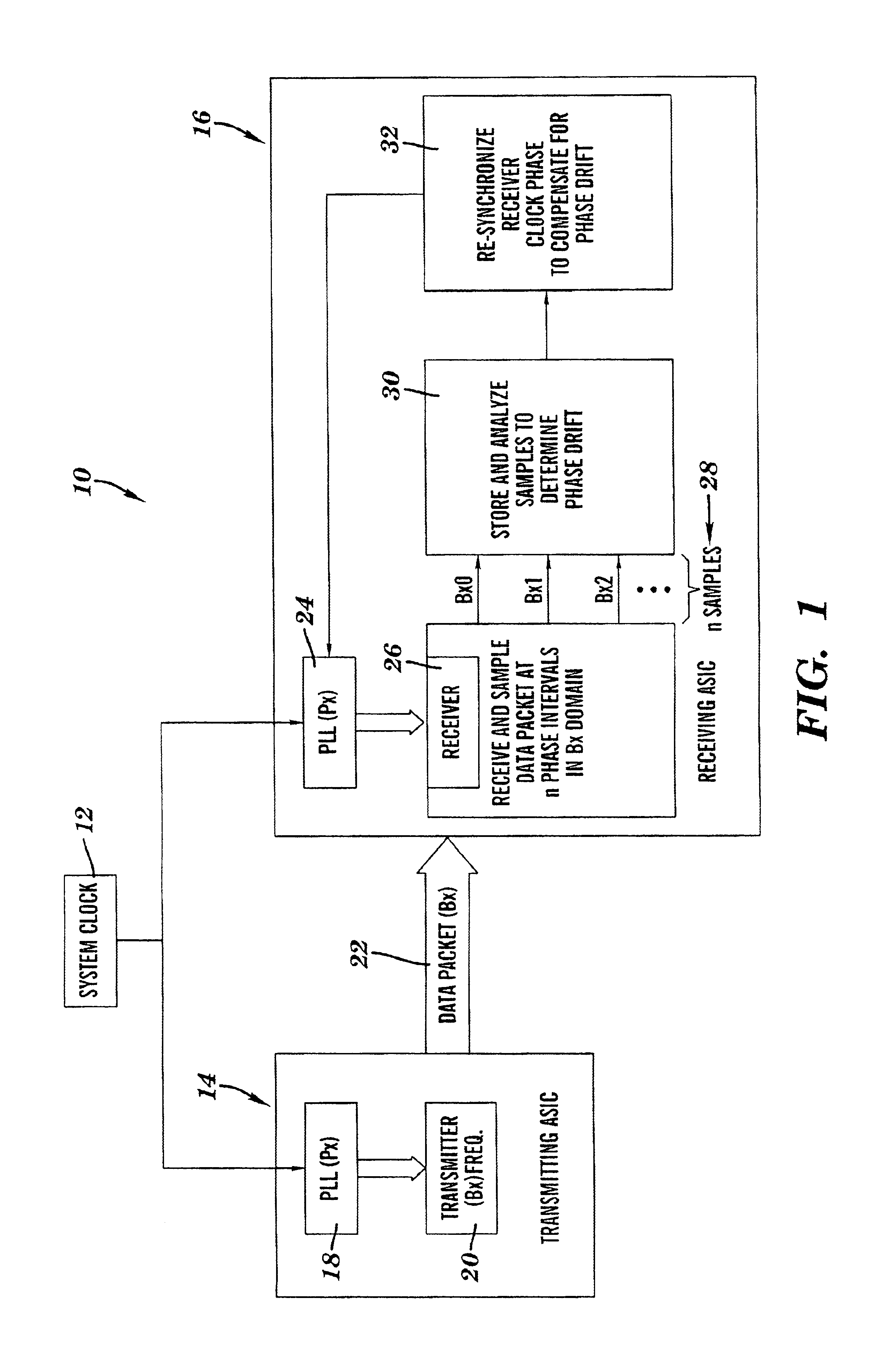
[0035]This invention is intended to address the high speed ASIC to ASIC serial data transmission problem as discussed above. An objective objective in developing this architecture is to maximize the realizable bit rate per package I / O, while minimizing the number of PLLs required per ASIC. Other secondary objectives are to: (1) maintain a high degree of tolerance of receiver clock to data jitter, and data pulse width variations; (2) eliminate any inherent requirement to balance link to link transmitter to receiver phase delays in a multiple link implementation; (3) provide a means to compensate for transmitter to receiver phase delay drift over time; and (4) develop a design whose transmission rate is only bounded by the upper end at which the process technology can operate, having no other inherent process, voltage, temperature, or frequency limitations. There are many challenges to accomplishing the above goals. However, the basic problem in achieving the goal of highes...


PUM


Abstract

A high speed serial interface system that compensates for phase drift by over sampling received data packets. The system utilizes a transmitter and receiver that operate within the same clock domain to achieve a frequency lock between the two devices. The receiver receives and samples each data packet at n phase intervals, stores and analyzes the samples to determine phase drift, and resynchronizes the receiver clock to compensate for phase drift on an ongoing basis.

Description

BACKGROUND OF THE INVENTION[0001]1. Technical Field[0002]The present invention relates to high speed digital communication systems, and more specifically to a high speed serial interface for ASIC to ASIC data transmissions.[0003]2. Background Art[0004]In high speed digital systems, it is often necessary to send digital information between discrete Integrated Circuit (IC) packages. Often, this issue becomes the critical bottleneck in overall system performance. This is readily apparent when considering communications systems where the overall throughput of the system (also referred to as the bandwidth of the system) is a fundamental limitation in determining how successfully the system can perform its intended application. One solution for increasing bandwidth is to design systems with more input / output (I / O) hardware to increase throughput. However, increasing the hardware requirements has a direct impact on cost in that the lower the overall bandwidth of a given IC package, the mor...

Claims


Application Information

Patent Timeline
Patent Type & Authority Patents(United States)
IPC IPC(8): H04L7/04H04L7/10
CPCH04L7/041H04L7/10
Inventor WILSON, THOMAS J.
Owner MEDIATEK INC
Learn More