Wafer scale production of optical elements

a technology of optical elements and scales, applied in the field of wafer scale production of optical elements, can solve the problems of high production cost of such etalons, inability to achieve desired properties, and inability to meet the requirements of production, so as to achieve precise optical performance characteristics, low production cost, and good production flexibility

Inactive Publication Date: 2005-05-24
II VI DELAWARE INC
View PDF13 Cites 12 Cited by
  • Summary
  • Abstract
  • Description
  • Claims
  • Application Information

AI Technical Summary

Benefits of technology

[0027]Optical elements comprising stacked, optically coupled etalon wafers (and / or diced components thereof) as disclosed above and the methods disclosed for their production will be recognized by those skilled in the art to represent a significant technological advance. Robust stacked, optically coupled etalon wafers can be produced meeting precise optical performance characteristics, with advantageously low production costs and good production flexibility. In preferred embodiments, the stacked, optically coupled etalon wafers have the advantageous attributes of small size, simple and potentially inexpensive construction, and good optical performance, including low loss, low polarization dependent loss and polarization mode dispersion, and low chromatic dispersion. Additional features and advantages will be understood from the following detailed description of certain preferred embodiments.

Problems solved by technology

Sputtering or other physical vapor deposition of the relatively thick cavity layer is time consuming and, therefore adds substantial time and cost to the production of such etalons.
The result is undesirably high cost for production for such etalons.
It has long been a recognized problem in this industry, that producing etalons having desired properties can be difficult and expensive.
In addition, there are industry-recognized problems associated with producing structurally robust etalons having desired, precise optical properties.
It is a disadvantage that adjustable etalons as in Ip involve considerable assembly complexity and cost.
Also, maintaining strict parallelism between the end plates can present additional difficulties.
The prior known optical etalons, as noted above, fail to fully meets the needs of many applications, especially for optical elements intended for optical communication systems, precision sensors, etc.

Method used


Image

  • Wafer scale production of optical elements
  • Wafer scale production of optical elements
  • Wafer scale production of optical elements

Examples


Embodiment Construction

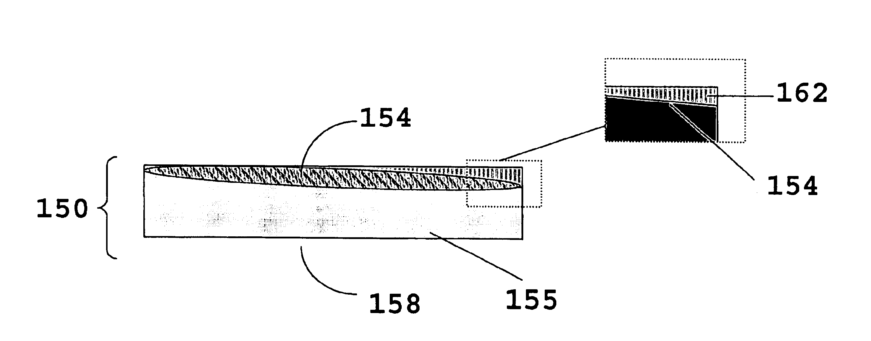
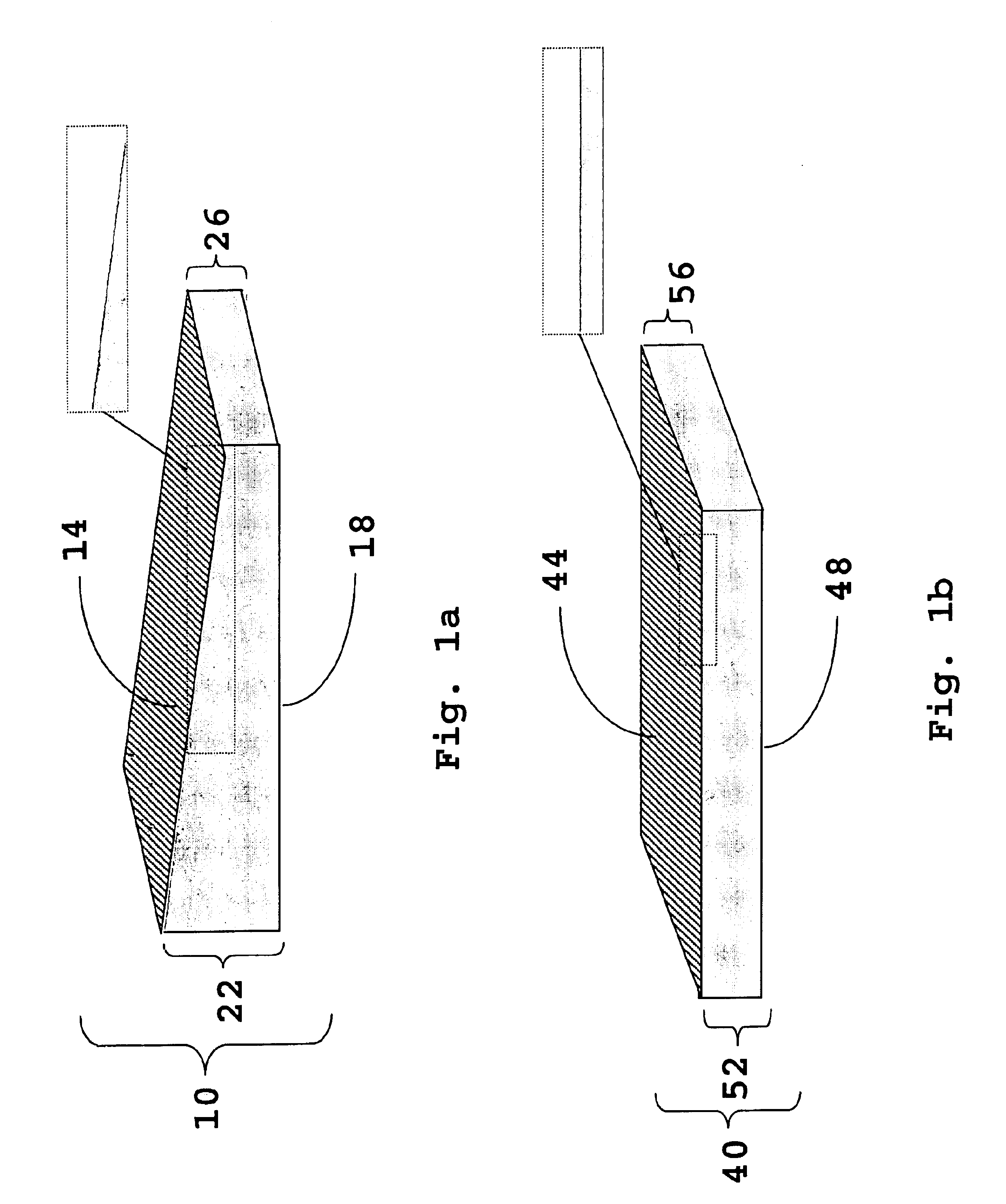
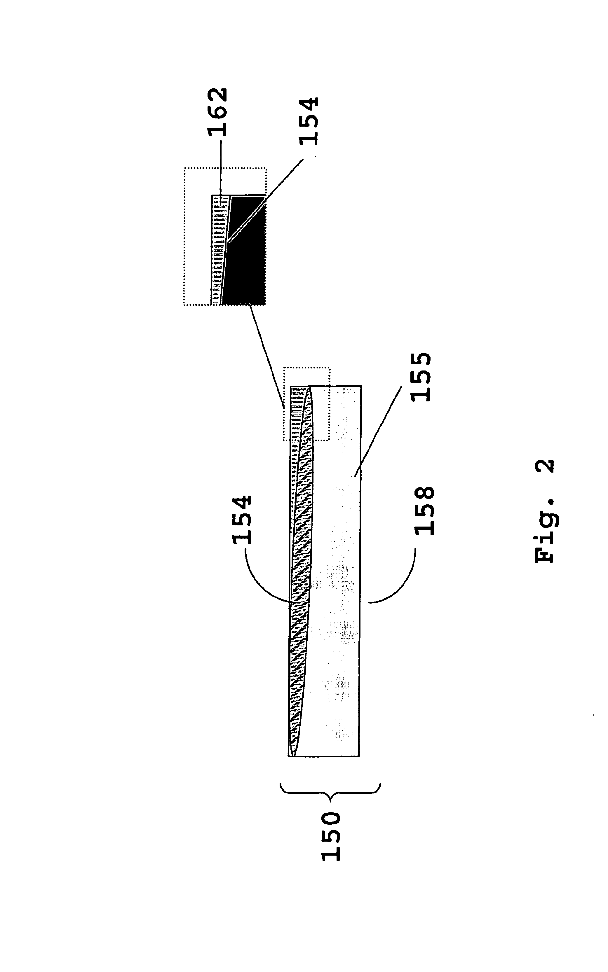
[0040]It will be recognized from the above, that the novel optical element wafers disclosed here can be formed in innumerable different configurations and sizes. The precise size and configuration of the optical element wafers, including the dimensions of the wafers, the choice of materials, design of the Fabry-Perot thin films, cavity spacing and the like will depend in large part on the particular application and use environment for which it is intended and its desired optical properties and performance characteristics. For convenience in this more detailed description of certain preferred embodiments, the diced components, either coupons or individual components, of the optical element wafers will generally be of a type suitable for use in optical elements of a fiber optic telecommunication system. It will be within the ability of those skilled in the art, however, given the benefit of this disclosure, to select suitable materials and designs, as well as manufacturing techniques,...


PUM

PropertyMeasurementUnit
diameteraaaaaaaaaa
thicknessaaaaaaaaaa
thicknessaaaaaaaaaa

Abstract

Improved optical element wafers comprising stacked, optically coupled etalon wafers are disclosed. Each etalon wafer comprises a bulk optic wafer defining the optic cavity between selectively transparent thin film mirror coatings. The bulk optic wafer comprises an optically transparent body, such as a portion of a substrate wafer, along with a wedge correcting coating on at least one of the two surfaces of the optically transparent body and / or a thickness-adjustment layer on one or both surfaces. The bulk optic wafer is a solid, self-supporting body, optically transparent (at the wavelength or wavelengths of interest), whose thickness, i.e., the dimension between the selectively transparent surfaces, defines the cavity spacing of the bulk optic etalon wafer. Methods of making and using the optical element wafers are also disclosed.

Description

PRIORITY APPLICATION[0001]This application claims the benefit of U.S. Provisional Application No. 60 / 276,020 filed on Mar. 15, 2001 and titled “Wafer Scale Production of Optical Elements.”CROSS-REFERENCED APPLICATIONS[0002]This application is related to commonly assigned U.S. Provisional Application No. 60 / 275,939 filed on Mar. 15, 2001 and titled “Apparatus and Method for Vacuum Coating Deposition,” U.S. Provisional Application No. 60 / 276,022 filed on Mar. 15, 2001 and titled “Optical System With 1×N Interleaver and Methods of Making and Using Same,” U.S. Provisional Application No. 60 / 275,918 filed on Mar. 15, 2001 and titled “Optical System With Cascaded Interleavers and Methods of Making and Using Same,” U.S. Provisional Application No. 60 / 276,018 filed on Mar. 15, 2001 and titled “Optically Coupled Etalons and Methods of Making and Using Same,” U.S. Provisional Application No. 60 / 275,920 filed on Mar. 15, 2001 and titled “Iso-Optical Thermal Compensator and Methods of Making an...

Claims


Application Information

Patent Timeline
Patent Type & Authority Patents(United States)
IPC IPC(8): G01J3/12G01J3/26G02B5/28G02B6/34
CPCG01J3/26G02B5/284G02B5/288Y10T428/2462G02B6/29358
Inventor SCOBEY, MICHAEL A.GHISLAIN, LUCIEN P.DERICKSON, DENNIS J.STOKES, LOREN F.
Owner II VI DELAWARE INC
Why Eureka
Try Eureka