

Negative-working photoresist composition
a technology of photoresist composition and negative working, applied in the direction of photosensitive materials, instruments, photomechanical equipment, etc., can solve the problems that the above-described type of photoresist composition cannot be quite satisfactory, and achieve excellent orthogonal cross sectional profile, low swellability, and high transparency
- Summary
- Abstract
- Description
- Claims
- Application Information
AI Technical Summary
Benefits of technology
Problems solved by technology
Method used
Image

Examples
example 1
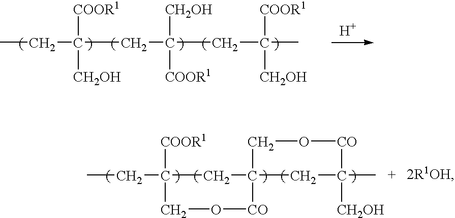
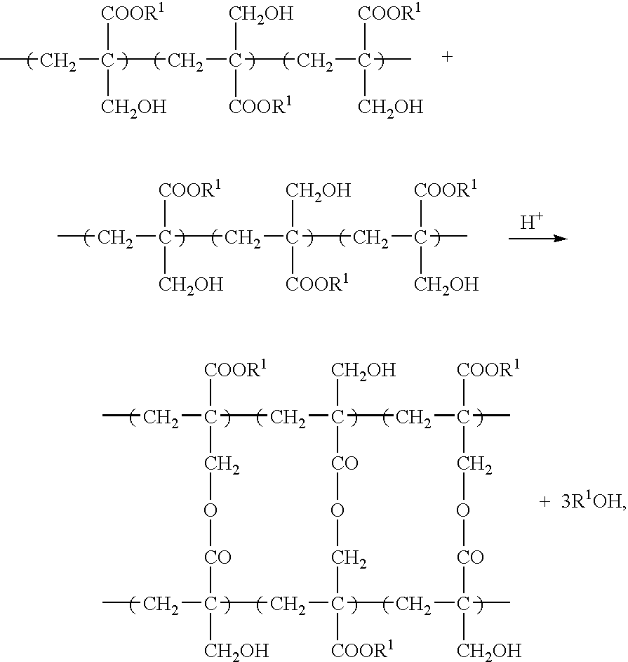
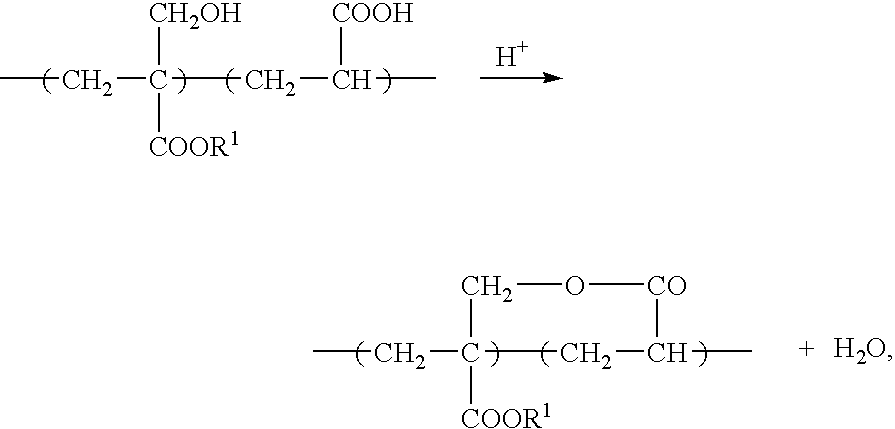
[0053]A negative-working photoresist solution was prepared by dissolving 100 parts of the Polymer 1 prepared in Preparation 1 and 3 parts of triphenylsulfonium trifluoromethanesulfonate in 670 parts of propyleneglycol monomethyl ether.
[0054]A semiconductor silicon wafer was coated with this photoresist solution by using a spinner followed by a drying and pre-baking treatment for 90 seconds on a hot plate at 120° C. to form a photoresist layer having a thickness of 0.5 μm. The photoresist layer was pattern-wise exposed to ArF excimer laser beams of 193 nm wavelength on an ArF exposure machine (manufactured by Nikon Co.) followed by a post-exposure baking treatment at 150° C. for 30 minutes and then subjected to a puddle development treatment at 23° C. for 65 seconds with a 2.38% by weight aqueous solution of tetramethylammonium hydroxide followed by rinse for 30 seconds with water and drying.
[0055]The exposure dose with the ArF excimer laser beams was taken as a measure of the photos...
example 2
[0056]The experimental procedure was substantially the same as in Example 1 excepting for replacement of the Polymer 1 with the same amount of the Polymer 2 prepared in Preparation 2.
[0057]The exposure dose as a measure of the sensitivity of the resist composition was 70 mJ / cm2 for the formation of a line-patterned resist layer of 0.40 μm line width. The patterned resist layer was free from swelling as examined on a scanning electron microscopic photograph for the cross sectional profile of the patterned resist layer.
example 3
[0058]The experimental procedure was substantially the same as in Example 1 excepting for replacement of the Polymer 1 with the same amount of the Polymer 3 prepared in Preparation 3.
[0059]The exposure dose as a measure of the sensitivity of the resist composition was 68 mJ / cm2 for the formation of a line-patterned resist layer of 0.30 μm line width. The patterned resist layer was free from swelling as examined on a scanning electron microscopic photograph for the cross sectional profile of the patterned resist layer.
PUM
| Property | Measurement | Unit |
|---|---|---|
| wavelength | aaaaa | aaaaa |
| thickness | aaaaa | aaaaa |
| wavelength | aaaaa | aaaaa |
Abstract
Description
Claims
Application Information