
Ceramic heater for semiconductor manufacturing/testing apparatus

a ceramic heater and semiconductor technology, applied in the direction of ohmic resistance heating, hot plate heating arrangement, electrical equipment, etc., can solve the problems of rapid temperature rise or temperature drop of resistance heating elements, and achieve the effect of ensuring temperature uniformity

Inactive Publication Date: 2005-05-24
IBIDEN CO LTD
View PDF10 Cites 14 Cited by
  • Summary
  • Abstract
  • Description
  • Claims
  • Application Information

AI Technical Summary

Benefits of technology

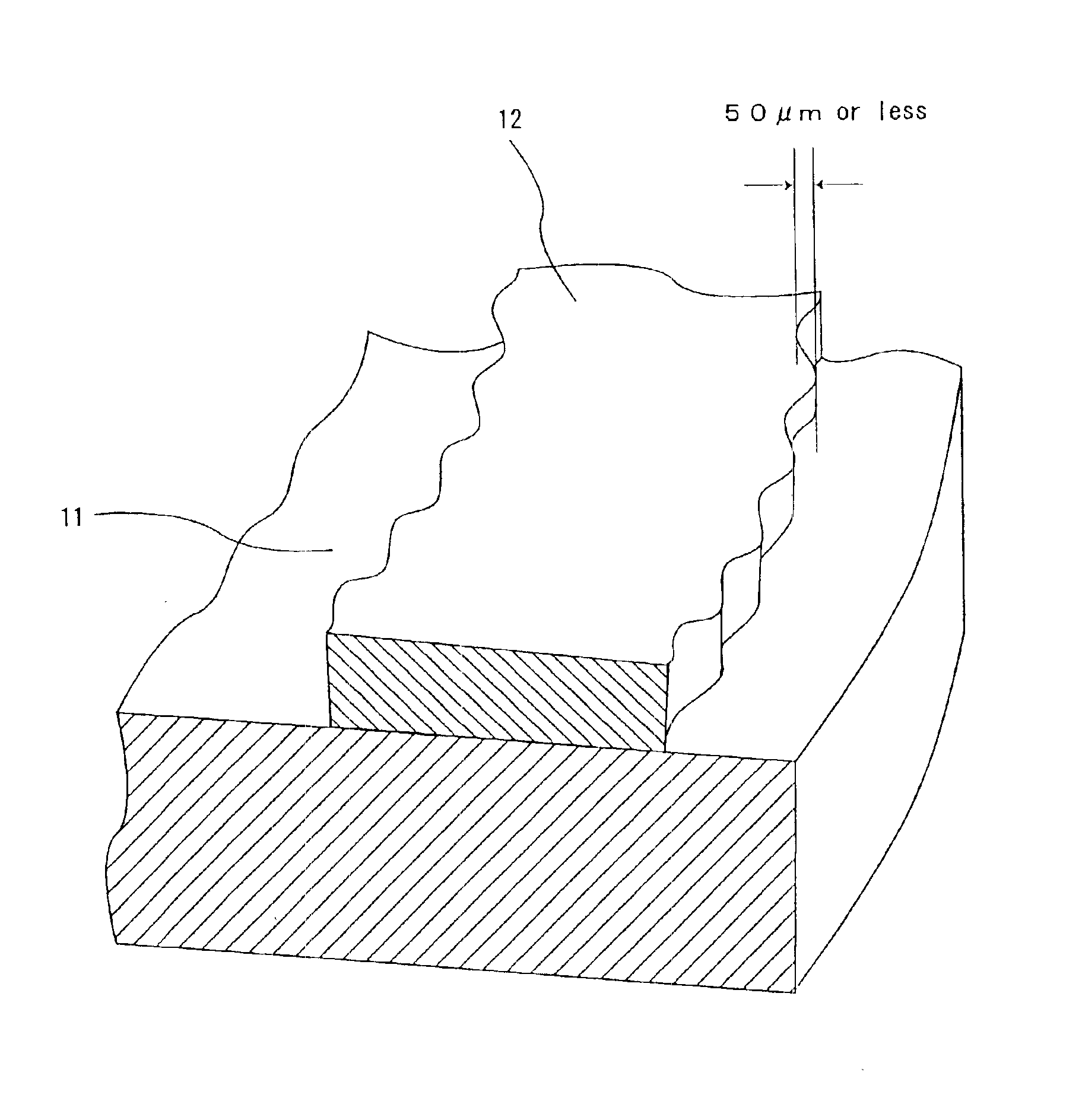
[0016]The size of the irregularities is desirably 0.05 μm or more. This is because the advantageous effects of the present invention are hardly produced if the size is less than 0.05 μm.
[0017]When the size of the irregularities is from 0.05 to 100 μm, extreme flow of air between circuits is suppressed. Therefore, rapid temperature-drop does not occur so that the evenness of the temperature is ensured.
[0018]Furthermore, the present invention is effective for the case in which the resistance heating element is drawn as a curve pattern. In any straight line pattern, the problem of exfoliation is hardly occurred.
[0019]Moreover, in the case that at least one part of the resistance heating element is formed in parallel, flow of atmospheric gas such as air between the patterns of the heating element becomes a problem. Thus, the adjustment of the irregularities on the side face becomes effective.

Problems solved by technology

However, in the ceramic heater described in JP Kokai Hei 11-40330, the resistance heating elements are formed to be drawn as curves (concentric circles), so that a problem that the resistance heating elements exfoliate by rapid temperature-rise or rapid temperature-drop is found.

Method used


Image

  • Ceramic heater for semiconductor manufacturing/testing apparatus
  • Ceramic heater for semiconductor manufacturing/testing apparatus
  • Ceramic heater for semiconductor manufacturing/testing apparatus

Examples


example 1

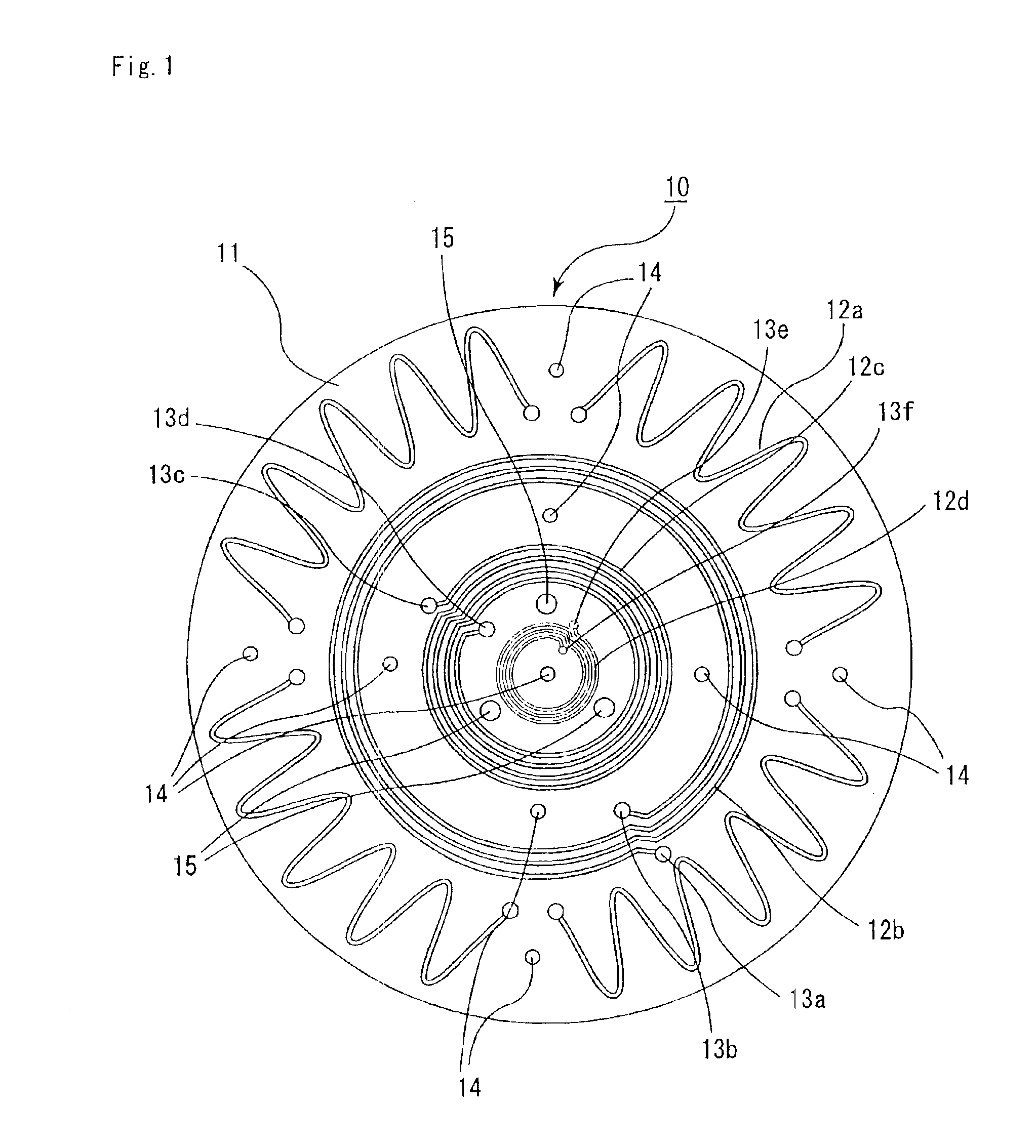
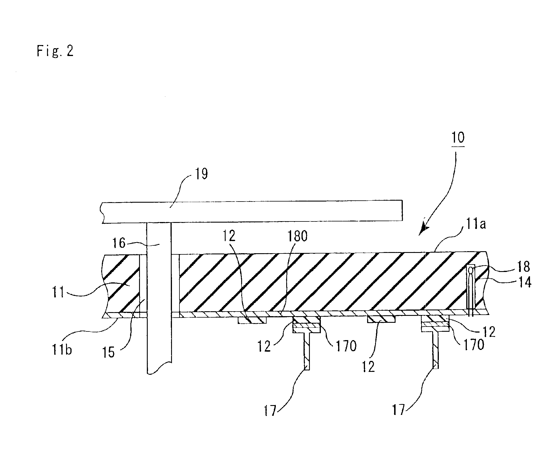
Manufacturing of a Ceramic Heater Made of SiC (FIGS. 1 and 2)

[0122](1) A composition comprising 100 parts by weight of SiC powder (average particle diameter: 0.3 μm), 4 parts by weight of B4C as a sintering aid, 12 parts by weight of an acrylic binder and an alcohol was subjected to spray-drying to prepare granular powder.

[0123](2) Next, this granular powder was put into a mold and formed into a flat plate form to obtain a raw formed body (green)

[0124](3) The raw formed body subjected to the working processing was degreased and then hot-pressed at 2100° C. and a pressure of 18 MPa to obtain a plate made of SiC and having a thickness of 3 mm.

[0125]Next, a surface of this plate was cut out into a disc having a diameter of 210 mm and the surface thereof was ground into a mirror plane until the Ra thereof became 0.1 μm. In this way, a ceramic substrate 11 was prepared.

[0126](4) Next, a sol solution prepared by hydrolyzing and polymerizing a mixed solution of 25 parts by weight of tetrae...

example 2

Manufacturing of a Hot Plate Made of AlN (FIGS. 1 and 2)

[0137](1) A composition comprising 100 parts by weight of aluminum nitride powder (made by Tokuyama Co., average particle diameter: 1.1 μm), 4 parts by weight of yttrium oxide (Y2O3: yttria, average particle diameter: 0.4 μm), 11.5 parts by weight of an acrylic binder, an alcohol was subjected to spray-drying to prepare granular powder.

[0138](2) Next, this granular powder was put into a mold having a hexagonal section and formed into a hexagonal flat plate shape to obtain a raw formed body(green).

[0139](3) The raw formed body subjected to the above processing was degreased and then hot-pressed at 1800° C. and a pressure of 20 MPa (200 kg / cm2) to obtain an aluminum nitride sintered body having a thickness of 3 mm.

[0140]Next, this sintered body was cut out into a disc having a diameter of 210 mm. In this way, a plate made of the ceramic (ceramic substrate) was prepared.

[0141]Thereafter, a sol solution was used in the same way as ...

example 3

[0150]A ceramic heater was manufactured in accordance with the method of Example 2. The size of irregularities of the opening in the screen printing plate was set to 110 μm.


PUM

PropertyMeasurementUnit
sizeaaaaaaaaaa
sizeaaaaaaaaaa
sizeaaaaaaaaaa

Abstract

A ceramic beater for a semiconductor producing / examining device having a resistance heating element superior in adhesion to a substrate. The ceramic heater includes a ceramic substrate and a resistance heating element formed on the surface of the ceramic substrate. Further, irregularities are formed on the side face of the resistance heating element.

Description

TECHNICAL FIELD[0001]The present invention relates to a ceramic heater for a semiconductor producing / examining device, which is used mainly in the semiconductor industry.BACKGROUND ART[0002]Semiconductors are very important products necessary in various industries, and a semiconductor chip is produced, for example, by slicing a silicon monocrystal into a predetermined thickness to manufacture a silicon wafer, and then forming plural integrated circuits etc. on this silicon wafer.[0003]In the manufacturing process of this semiconductor chip, the silicon wafer put on an electrostatic chuck is subjected to various treatments such as etching and CVD, to form a conductor circuit, an element and so on. A resin for a resist is applied thereto and is then heated and dried.[0004]For such heating, a ceramic heater is used. JP Kokai Hei 11-40330 and so on disclose a ceramic heater in which a substrate made of a carbide ceramic or a nitride ceramic is used and resistance heating elements are fo...

Claims


Application Information

Patent Timeline
Patent Type & Authority Patents(United States)
IPC IPC(8): H01L21/00H05B3/22H05B3/14H05B3/26
CPCH01L21/67103H05B3/265H05B3/143
Inventor ITO, YASUTAKAMASHIMA, KAZUTAKA
Owner IBIDEN CO LTD
Learn More