Split and merge design flow concept for fast turnaround time of circuit layout design

Active Publication Date: 2005-05-24
BELL SEMICON LLC
View PDF1 Cites 235 Cited by
  • Summary
  • Abstract
  • Description
  • Claims
  • Application Information

AI Technical Summary

Benefits of technology

[0014]Splitting the database into a physical database and a timing database and processing both databases concurrently (one for routing and timing and the other for physical verification) improves the turnaround time of the de

Problems solved by technology

Describing a complex digital system with hundreds of thousands of gates at the gate level is an extremely challenging task, and therefore, high level synthesis tools were introduced.
For example, in FPGAs limited routing resources, routing channel congestion and routing delays must also be considered during the placement phase.
Serious problems could occur in model 100 if DRC/LVS started prior to completing the routing and timing.
These serious problems would arise due to mistakes in the physical implementation that would be discovered very late in the design process.
Discovering a serious problem late in the design process

Method used


Image

  • Split and merge design flow concept for fast turnaround time of circuit layout design
  • Split and merge design flow concept for fast turnaround time of circuit layout design
  • Split and merge design flow concept for fast turnaround time of circuit layout design

Examples


Embodiment Construction

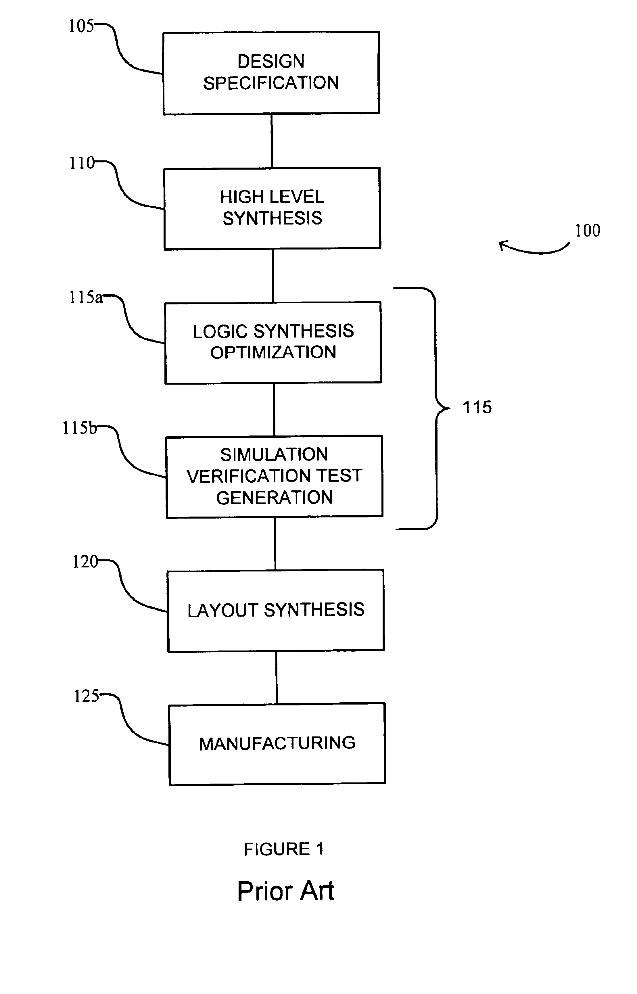
[0017]The present invention relates generally to manufacturing techniques for the design and development of mask-produced devices, and more specifically to improving a turnaround time between layout and final approval of a device specification (e.g., a GDS2 database). The following description is presented to enable one of ordinary skill in the art to make and use the invention and is provided in the context of a patent application and its requirements. Various modifications to the preferred embodiment and the generic principles and features described herein will be readily apparent to those skilled in the art. Thus, the present invention is not intended to be limited to the embodiment shown but is to be accorded the widest scope consistent with the principles and features described herein.

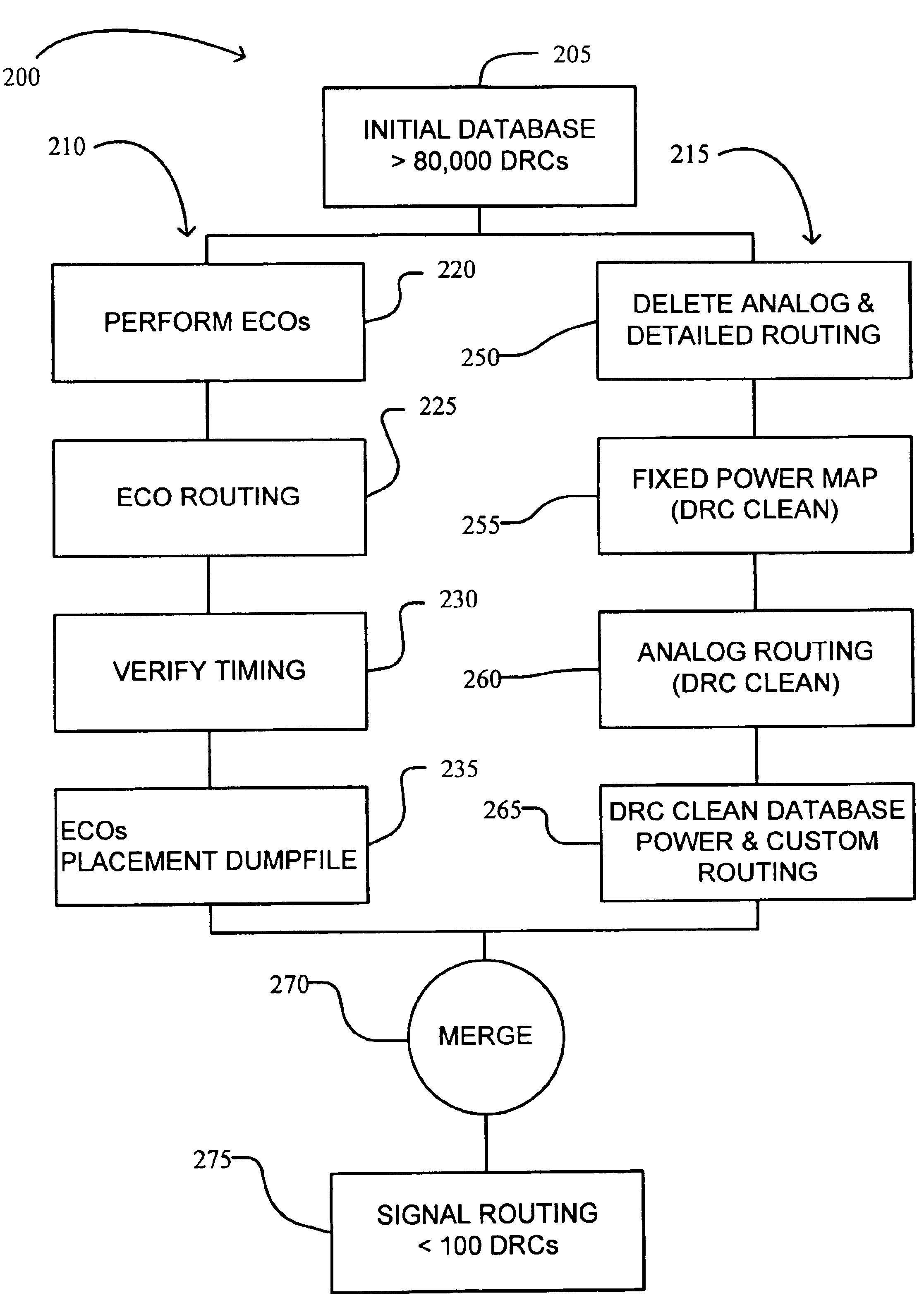
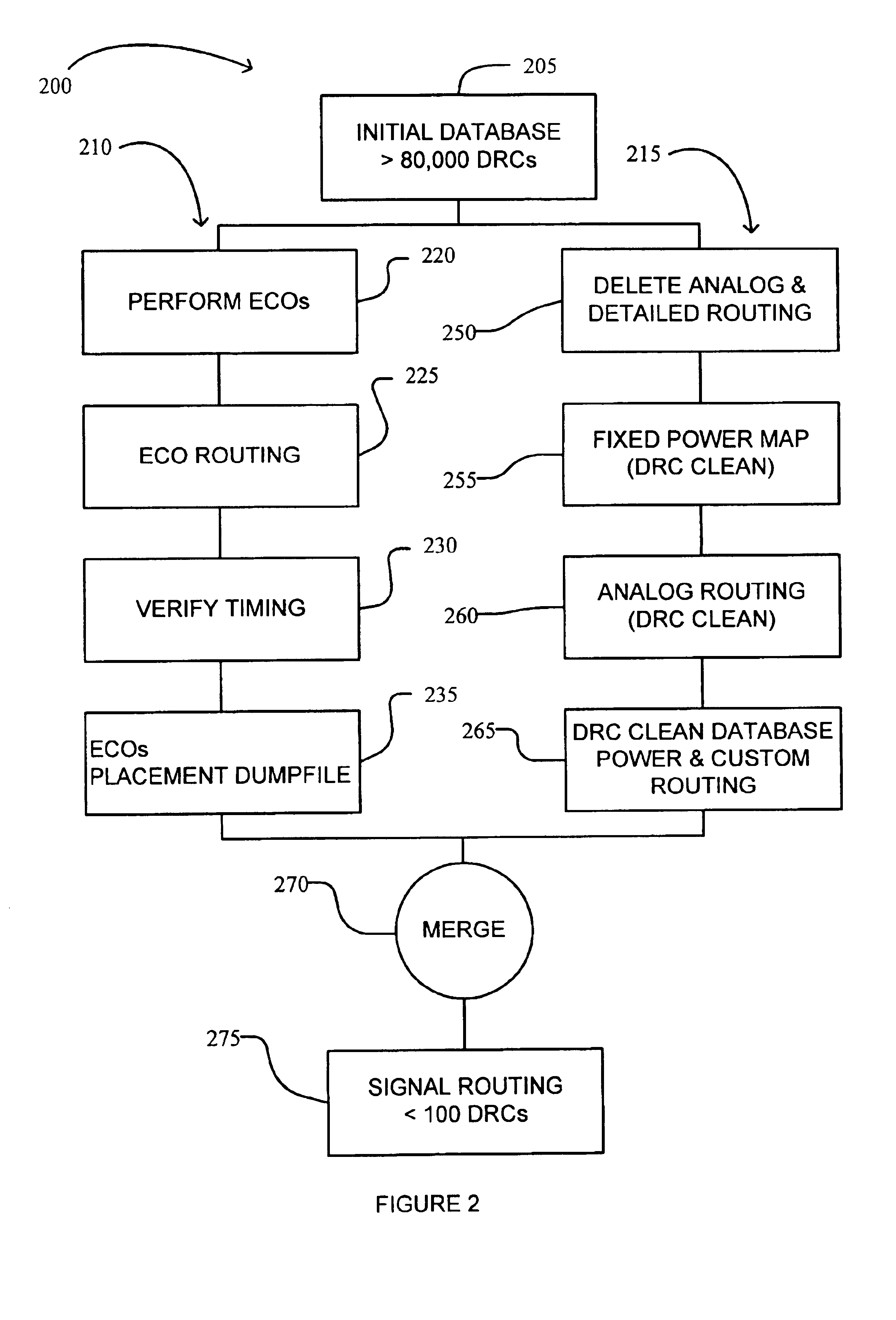
[0018]FIG. 2 is a preferred embodiment of a portion of a design cycle model 200 that improves turnaround time. Design cycle model 200 separates a layout database 205 into two database flows: a tim...


PUM


Abstract

A method and system is disclosed to improve the turnaround time to provide adequate time to meet project schedules in the event that adjustments or modifications to the design are necessary. A method for improving a turnaround time for design verification of a process database representing a semiconductor design includes the steps of (a) deriving a timing database and a (DNE) database from the process database; (b) performing, using the timing database, one or more design changes and one or more timing verifications and corrections to generate a modified timing database; (c) initiating, using the process database, physical validation of the semiconductor design prior to completion of step (b) to generate a modified DNE database; (d) merging the modified timing database with the modified DNE database to form a modified process database; and (e) performing, using the modified process database, one or more design verification checks of the semiconductor design.

Description

FIELD OF THE INVENTION[0001]The present invention relates generally to manufacturing techniques for the design and development of mask-produced devices, and more specifically to improving a turnaround time between layout and final approval of a device specification (e.g., a GDS2 database).BACKGROUND OF THE INVENTION[0002]The design, layout, test and manufacture of devices produced using masking processes like photolithography are very well known. For example, U.S. Pat. No. 6,171,731 (the '731 patent) issued to Medvedeva, et. al. entitled “Hybrid Aerial Image Simulation” provides a background for semiconductor fabrication. The specification of the '731 patent is hereby incorporated herein as though set forth in full by this reference.[0003]The classical approach to design an Application Specific Integrated Circuit (ASIC) either in a fixed monolithic semiconductor technology such as gate arrays (GA) or standard cells (SC) or in a programmable technology like Field Programmable Gate Ar...

Claims


Application Information

Patent Timeline
IPC IPC(8): G06F17/50
CPCG06F17/5031G06F30/3312
Inventor BOLUKI, HUMANMBOUOMBOUO, BENJAMINLEYRER, JOHANN
Owner BELL SEMICON LLC
Why Eureka
Try Eureka