Method for fabrication of field-effect transistor to reduce defects at MOS interfaces formed at low temperature

US6905920B2Inactive Publication Date: 2005-06-14138 EAST LCD ADVANCEMENTS LTD

Image

  • Method for fabrication of field-effect transistor to reduce defects at MOS interfaces formed at low temperature
  • Method for fabrication of field-effect transistor to reduce defects at MOS interfaces formed at low temperature
  • Method for fabrication of field-effect transistor to reduce defects at MOS interfaces formed at low temperature

Examples


Embodiment Construction

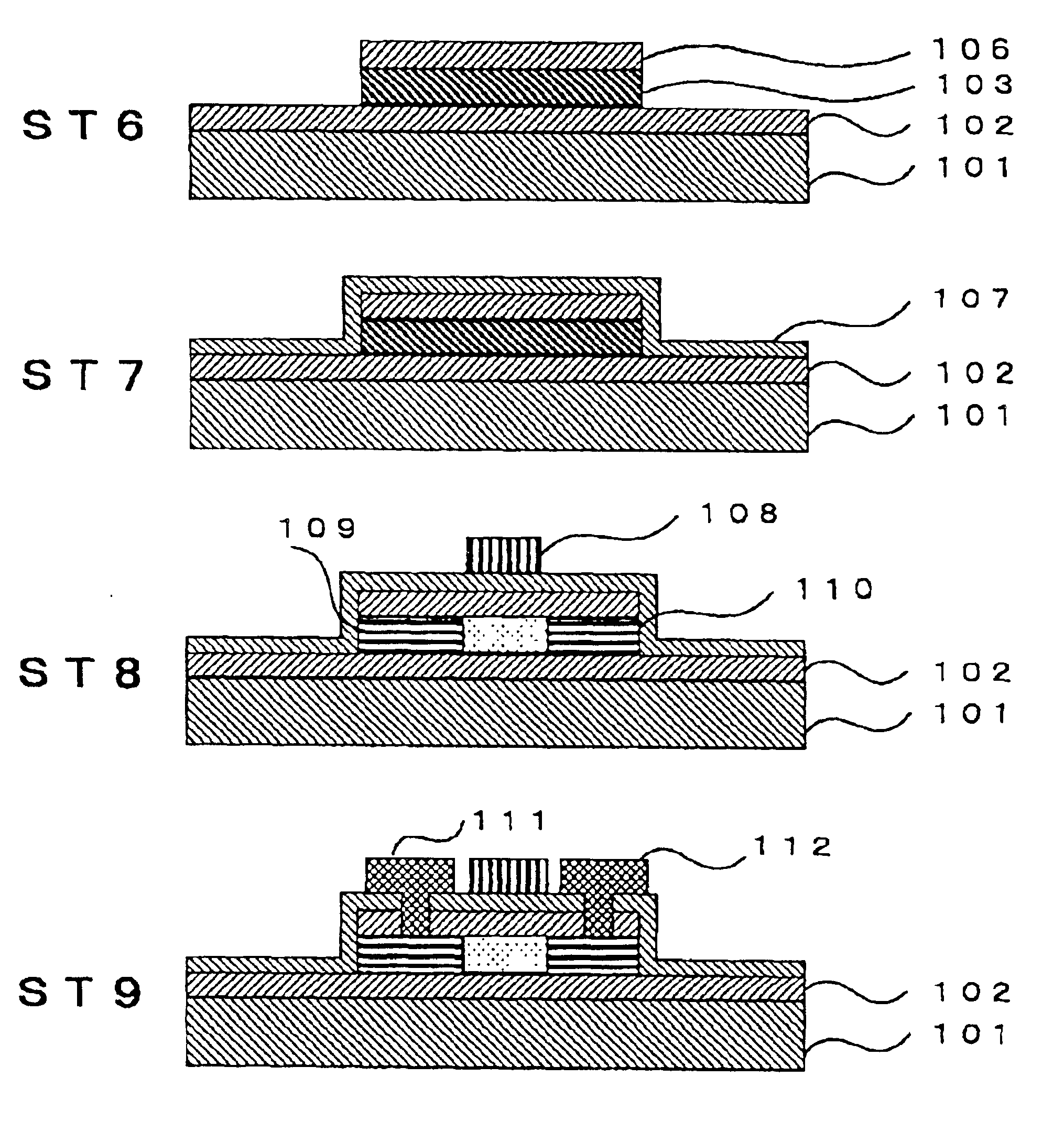
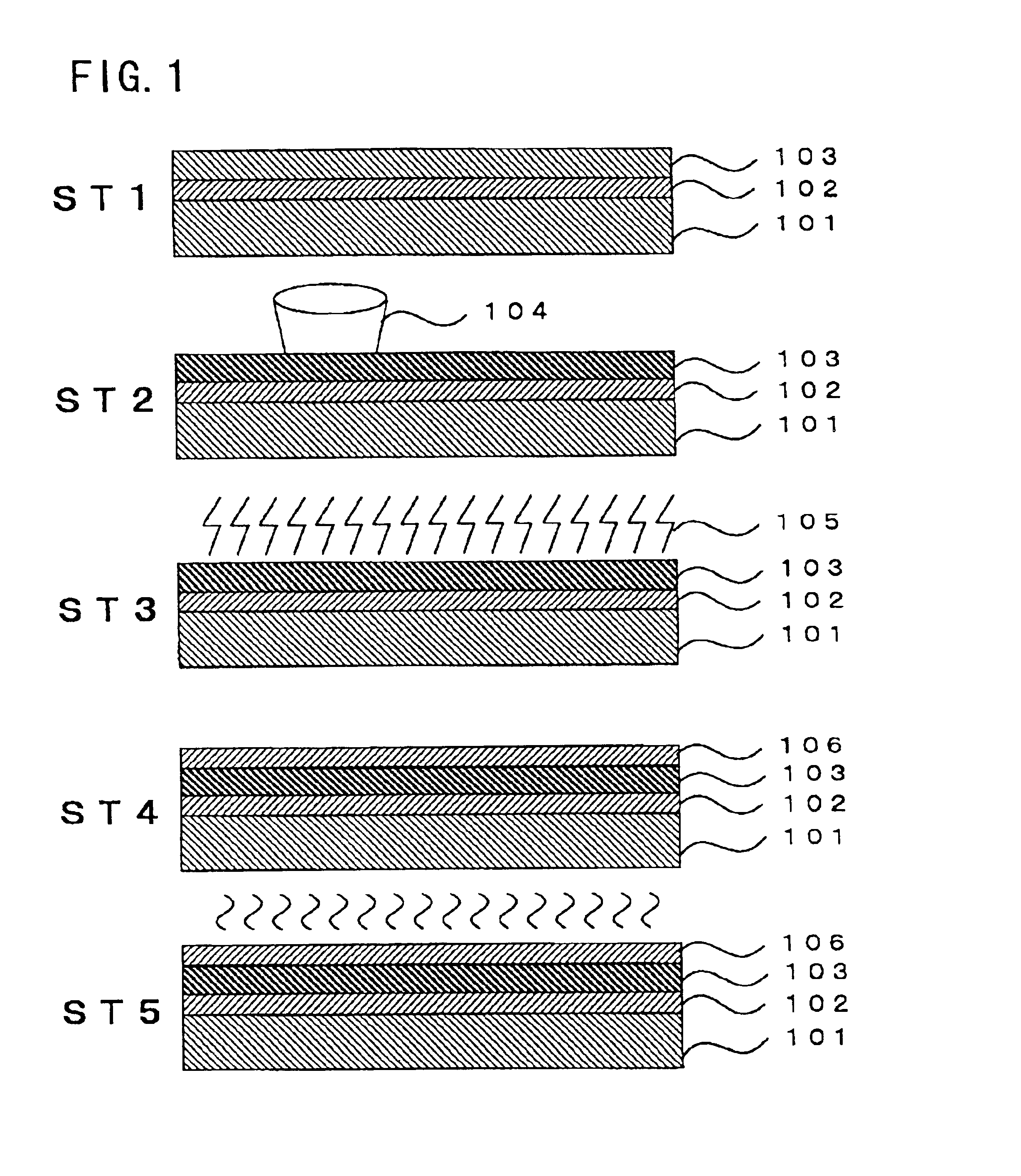
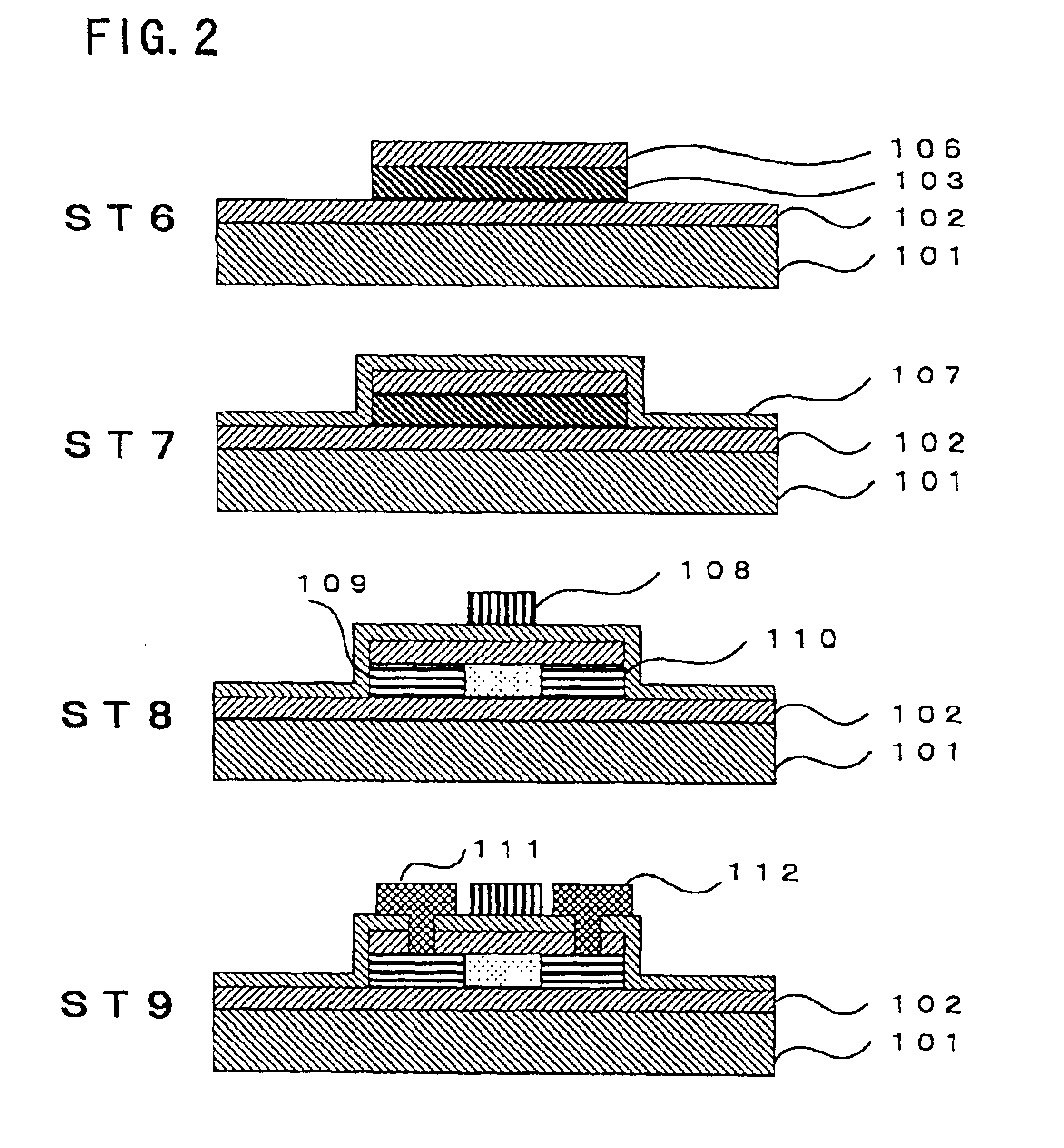
[0025]A preferred embodiment of the present invention will be described below with reference to the drawings attached. FIG. 1 and FIG. 2 are cross-sectional views illustrating the process for the fabrication of a polycrystalline silicon TFT.

Formation of Semiconductor Thin Film (FIG. 1: ST1)

[0026]In order to implement the present invention, usually a prime protective layer 102 is formed on a substrate 101 and then a semiconductor layer 103 is formed thereon. Accordingly, the formation method consisting of such operations will be described.

[0027]Examples of substrates 101 suitable in accordance with the present invention include: conductive materials such as metals; ceramic materials such as silicon carbide (SiC), alumina (Al2O3), aluminum nitride (AIN) and the like; transparent or opaque insulating substances such as fused quartz or glass; semiconductors such as silicon wafers and the like; and LSI substrates obtained by processing the above-mentioned materials. The semiconductor lay...


PUM


Abstract

A method for the fabrication of a field-effect transistor wherein after forming a semiconductor layer serving as an active layer on a substrate, the substrate temperature is set at no higher than 100° C., a gate insulating film is formed on the semiconductor layer. Then, the gate insulating film is heat treated in an atmosphere containing water. By heat treating in the atmosphere containing water, OH bonds in the vicinity of the insulating film interface are reduced and, therefore, the CV characteristic thereof is improved.

Description

BACKGROUND OF THE INVENTION[0001]1. Field of Technology[0002]The present invention relates to a method for the fabrication of thin-film transistors employed as elements which are formed on a single-crystal substrate, for example, field-effect transistors, thin-film transistors formed on an insulator, logic circuits formed therefrom, and a structural component of display drive circuits or display pixels used in electronic apparatuses such as memory circuits, liquid-crystal displays, and organic EL displays.[0003]2. Description of the Related Art[0004]Semiconductor films such as polycrystalline silicon films have been widely used in thin-film transistors (abbreviated as TFT hereinbelow) or solar cells. In particular, polycrystalline silicon (poly-Si) TFT can be produced on a transparent insulating substrate such as glass substrate, while allowing for increased mobility. Polycrystalline silicon TFTs have been widely used as light modulating elements, for example, in liquid-crystal disp...

Claims


Application Information

Patent Timeline
14 Jun 2005
Publication
US6905920B2
IPC
H01L21/336; H01L29/786; H01L21/02; H01L29/66; H01L29/49; H01L29/40; H01L21/316
CPC
H01L29/4908; H01L29/78684; H01L29/78681; H01L29/66757
Inventors
HIGASHI, SEIICHIRO; ABE, DAISUKE