Semiconductor apparatus fabrication method forming a resist pattern, a film over the resist, and reflowing the resist

a technology of semiconductor apparatus and resist pattern, applied in the direction of semiconductor devices, electrical apparatus, photosensitive material processing, etc., can solve the problems of resist pattern not only in individual patterns, but also insufficient exposure at the bottom of resist, etc., and achieve the effect of overcoming edge roughness and avoiding the formation of resist patterns

Inactive Publication Date: 2005-06-14
FUJITSU SEMICON LTD
View PDF6 Cites 10 Cited by
  • Summary
  • Abstract
  • Description
  • Claims
  • Application Information

AI Technical Summary

Benefits of technology

[0014]It is a general object of the present invention to provide a novel and useful semiconductor apparatus fabrication method in which the above-mentioned problems are eliminated.

Problems solved by technology

As a result, there arises insufficient exposure at the bottom of the resist.
However, when a pattern to be formed has an even narrower width of 0.05 μm or 0.01 μm, a resist pattern cannot have a stable edge in terms of not only individual patterns but also the interior of one pattern due to a light contrast problem on exposure or a resist composition nonuniformity problem.
However, it is difficult to overcome edge roughness by simply improving resist materials with respect to current ultra-micro semiconductor apparatuses in which the pattern size is less than 0.1 μm.
However, if the resist pattern is heated, there is a risk that the resist pattern will be deformed as a whole.
However, it is difficult to prepare an illuminant suitable to such wavelength.
In this conventional technique, however, if the softening temperature does not sufficiently decrease, the reflow arises not only on the pattern surface but also throughout the entire pattern.
In this case, however, it is impossible to avoid reduction of the pattern size.
As a result, it is necessary to perform exposure at the limit of exposure resolution, and there arise serious problems on the yield and the throughput.
As mentioned above, no effective method for improving the edge roughness of a fine resist pattern has been proposed.

Method used


Image

  • Semiconductor apparatus fabrication method forming a resist pattern, a film over the resist, and reflowing the resist
  • Semiconductor apparatus fabrication method forming a resist pattern, a film over the resist, and reflowing the resist
  • Semiconductor apparatus fabrication method forming a resist pattern, a film over the resist, and reflowing the resist

Examples


first embodiment

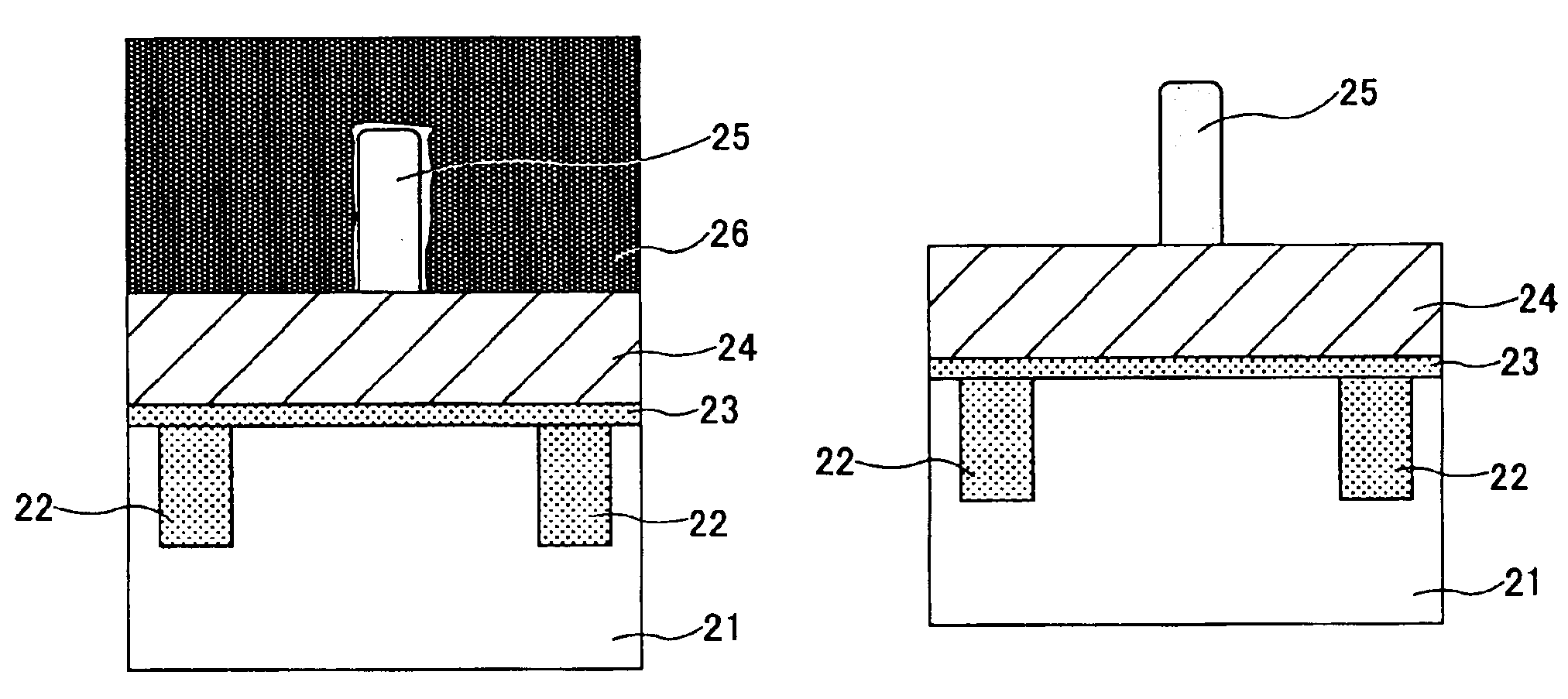
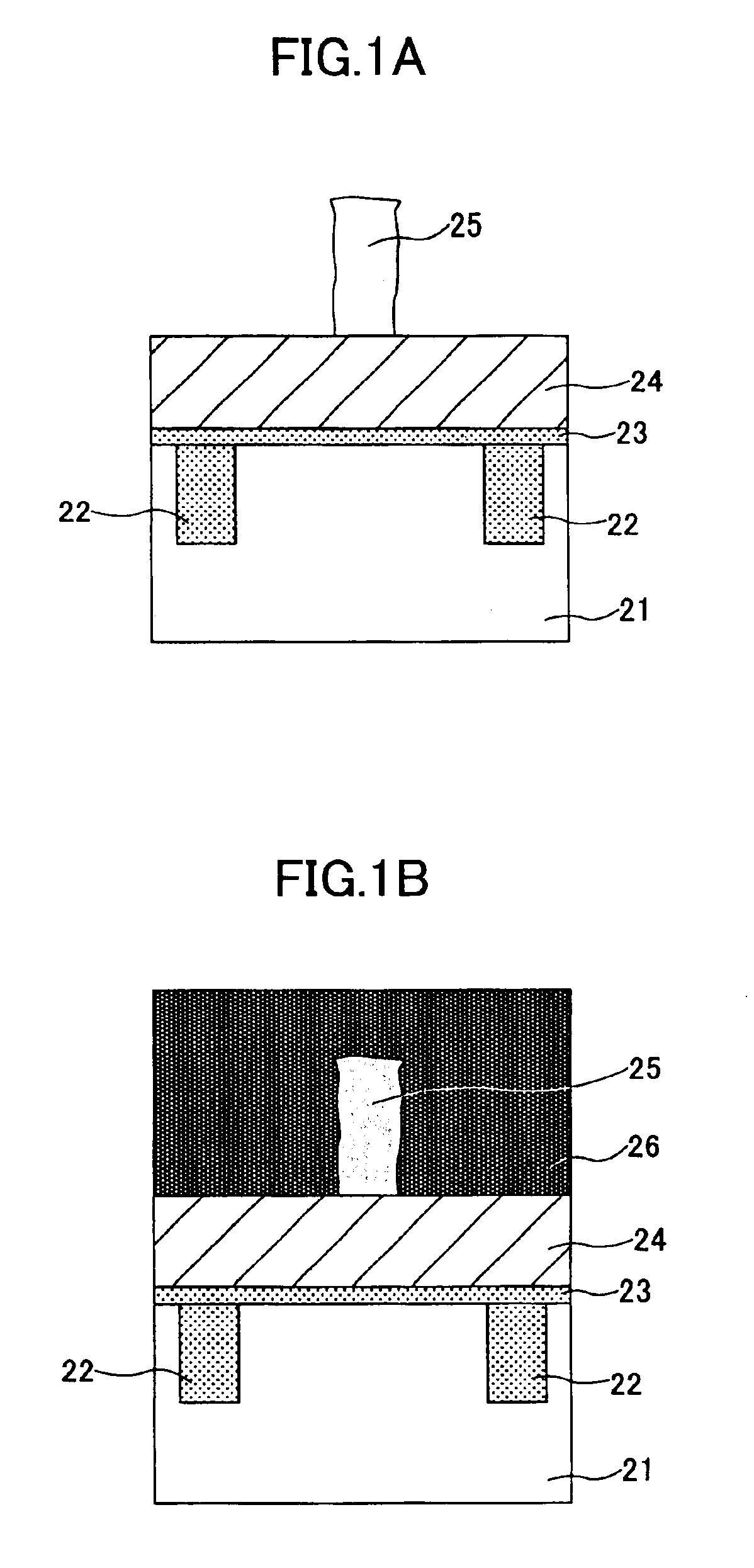
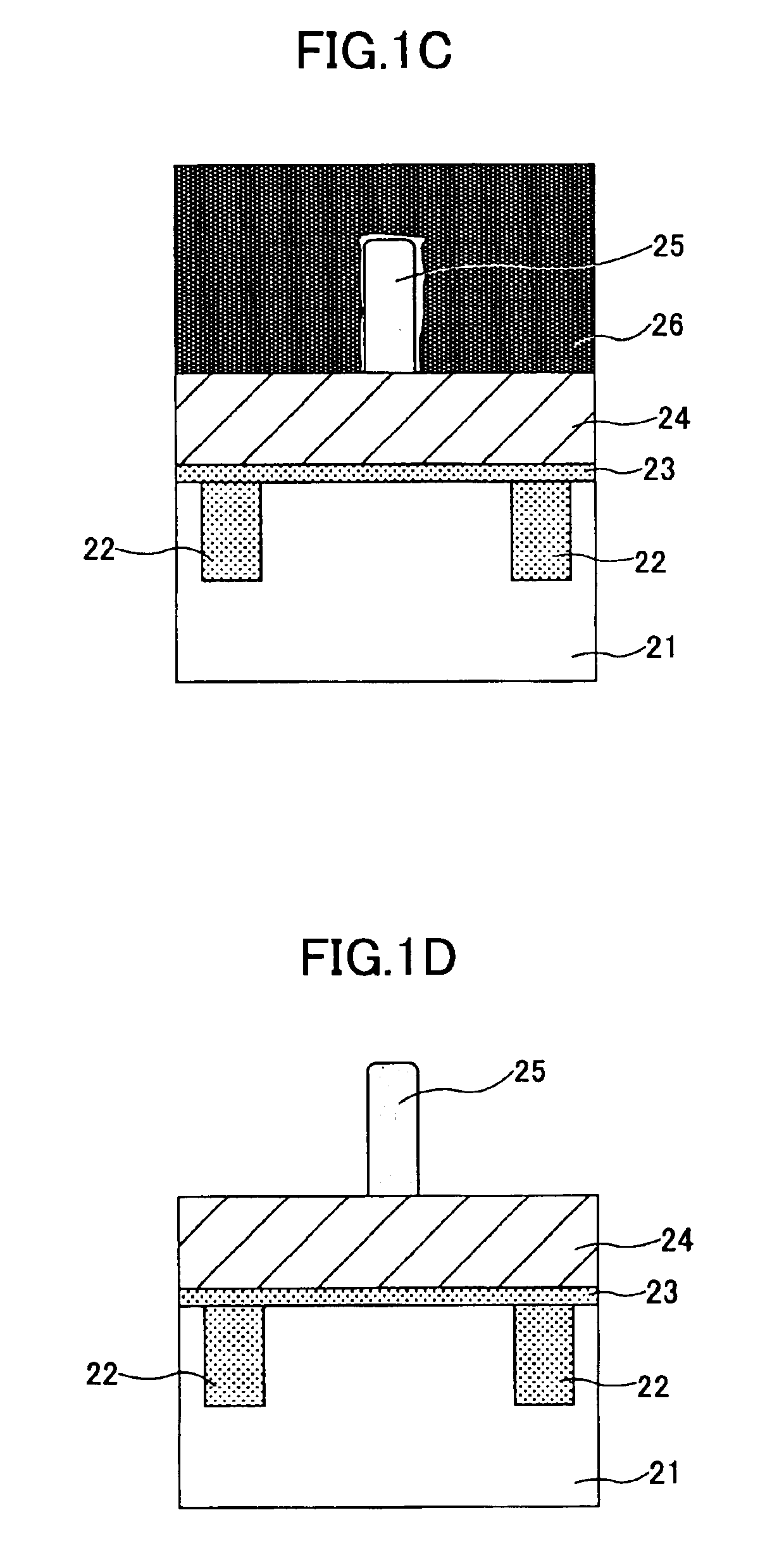
[0042]A description will now be given, with reference to FIGS. 1A through 1F, of a semiconductor apparatus fabrication method according to the present invention.

[0043]Referring to FIG. 1A, an element separation area 22 and an insulation film 23, which serves as a gate insulation film, are formed on a silicon substrate 21. In addition, a polysilicon film 24 is formed on the insulation film 23 as a gate electrode.

[0044]In a process illustrated in FIG. 1A, a chemically amplified resist is formed on the polysilicon film 24 via an organic or an inorganic antireflection film, which is not illustrated in FIG. 1A. Then, when the chemically amplified resist is exposed and developed, it is possible to form a resist pattern 25 corresponding to the desired gate electrode pattern.

[0045]For instance, such a chemically amplified resist may be formed of an ArF chemically amplified resist PAR-101 manufactured by Sumitomo Chemical Co., Ltd. In this case, the ArF chemically amplified resist PAR-101 is...

second embodiment

[0061]A description will now be given, with reference to FIG. 3A through 3F, of a semiconductor apparatus fabrication method according to the present invention wherein the same parts as those parts described above are designated by the same reference numerals and the description thereof is omitted.

[0062]Referring to FIG. 3A, the semiconductor apparatus fabrication method according to the second embodiment provides a silicon oxide film 35, which is used as a hard mask, on the polysilicon film 24 and provides an antireflection film 36 formed of an insulation film such as SiN on the silicon oxide film 35. Additionally, an adamantyl acrylate system chemically amplified resist film is formed on the antireflection film 36. When a high resolution exposure apparatus exposes and develops the adamantyl acrylate system chemically amplified resist film as in the first embodiment, a resist pattern 37 is formed.

[0063]As is shown in FIG. 3A, edge roughness arises in the resist pattern 37. In the s...

third embodiment

[0070]A description will now be given, with reference to FIGS. 4A through 4F, of a semiconductor apparatus fabrication method according to the present invention.

[0071]Referring to FIG. 4A, an element area is defined on a silicon substrate 41 by providing an element separation area 42, and a gate electrode 44 is formed in the element area on the substrate 41 via a gate insulation film 43. Furthermore, an n-type or p-type source extension area 41a is formed in one side of the gate electrode 44 on the substrate 41, and an n-type or p-type drain extension area 41b is formed in the other side.

[0072]The gate electrode 44 retains a silicide low resister layer 44A in the upper side thereof and sidewall insulation films 44S on the both sidewalls thereof. Furthermore, an n-type or p-type source diffusion area 41c and an n-type or p-type drain area 41d are provided in the exterior of the sidewall insulation films 44S in the silicon substrate 41.

[0073]An inter-layer insulation film 45 is provid...


PUM

PropertyMeasurementUnit
wavelengthaaaaaaaaaa
widthaaaaaaaaaa

Abstract

A semiconductor apparatus fabrication method is capable of effectively suppressing edge roughness when an extremely fine resist pattern is formed. In the semiconductor apparatus fabrication method, the extremely fine resist pattern is covered with a film whose heat-resistance temperature is higher than the softening temperature of the resist pattern. In this state, the resist pattern is heated at a temperature higher than the softening temperature and lower than the heat-resistance temperature in order to cause reflow in the resist pattern.

Description

CROSS-REFERENCE TO RELATED APPLICATIONS[0001]The present application is based on Japanese priority application No. 2002-245377 filed Aug. 26, 2002, the entire contents of which are hereby incorporated by reference.BACKGROUND OF THE INVENTION[0002]1. Field of the Invention[0003]The present invention generally relates to a semiconductor apparatus fabrication method, and more particularly to a semiconductor apparatus fabrication method that includes processes for forming an ultra fine pattern by using a resist pattern.[0004]2. Description of the Related Art[0005]Recent advances in micro-fabrication techniques have realized ultra high-speed semiconductor apparatuses in which patterns of a gate electrode and a contact hole are formed under an approximately 0.1 μm design rule. Currently, it is being considered to use a 0.05 μm design rule and further a 0.01 μm design rule. When such an ultra high-speed semiconductor apparatus is fabricated, a resist is formed on a film whereupon a pattern...

Claims


Application Information

Patent Timeline
Patent Type & Authority Patents(United States)
IPC IPC(8): G03F7/40H01L21/02H01L21/027H01L21/3213H01L21/311
CPCG03F7/40H01L21/0273H01L21/32139H01L21/31144Y10S438/945
Inventor ARITA, TOSHIYUKI
Owner FUJITSU SEMICON LTD
Why Eureka
Try Eureka