Method for improving planarity of shallow trench isolation using multiple simultaneous tiling systems

a technology of tiling system and shallow trench, which is applied in the direction of semiconductor devices, semiconductor/solid-state device details, electrical apparatus, etc., can solve the problems of inability to remove nitride, lack of planarity at this stage, and uneven cmp mechanism, etc., and achieve superior topography results

Inactive Publication Date: 2005-06-14
ADVANCED MICRO DEVICES INC
View PDF9 Cites 42 Cited by
  • Summary
  • Abstract
  • Description
  • Claims
  • Application Information

AI Technical Summary

Benefits of technology

[0021]Based in part in this realization, the invention broadly is a set of optimizing principles for placing tiles, realized by taking carefully into account the nature of any trench fill oxide deposition which allows the nitride pattern density to be decoupled from the oxide pattern density. When very small or narrow active features are coated with, for example, HDP oxide, the amount of oxide over the nitride is proportionally lower compared to the amount of oxide over nitride for a large active feature. Since the desired pattern density distribution can be different during the bulk planarization of oxide compared to the overpolish and nitride clearing portions of the CMP process, the invention realizes the advantageous of using, simultaneously, two (or more) different tiling methods to address the two (or more) different regimes.
[0022]Thus the invention in one aspect is a process that at the trench level surveys oxide density and nitride density over an entire wafer surfa

Problems solved by technology

A problem with CMP is that at places along a polished surface, the CMP mechanism has a tendency to create uneven, non-planar portions.
Both dishing and erosion can lead to more resistive interconnects and cause problems at subsequent CMP and photolithography steps due to the resulting lack of planarity.
Lack of planarity at this stage is often fatal to the wafer, as the following illustrates.
The nitride is stripped off after the CMP process is completed, using a hot phosphoric acid bath; but the nitride cannot be removed if there is any oxide remaining on top of it.
Residual nitride of this type will render the chip nonfunctional.
On the other end of the spectrum, if the nitride is completely polished away anywhere on the wafer, the active silicon will be exposed to the CMP process and become contaminated, again resulting in a nonfunctional chip.
These areas will result in residual nitride and render the device unusable.
Further, the oxide to active step var

Method used


Image

  • Method for improving planarity of shallow trench isolation using multiple simultaneous tiling systems
  • Method for improving planarity of shallow trench isolation using multiple simultaneous tiling systems
  • Method for improving planarity of shallow trench isolation using multiple simultaneous tiling systems

Examples


example 1

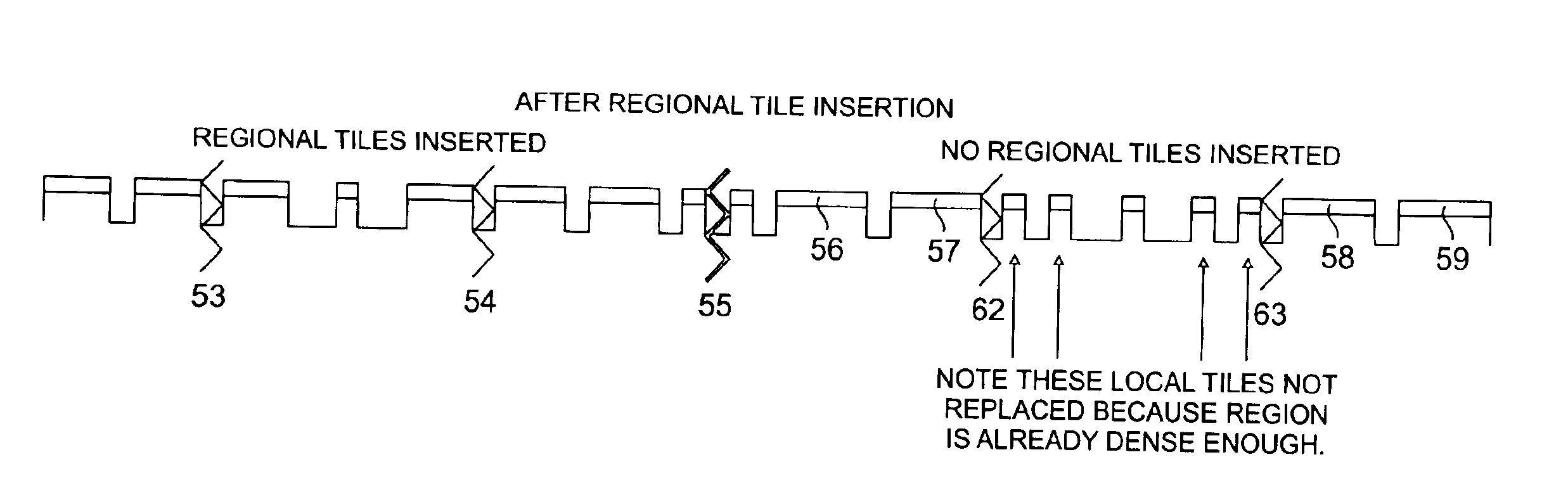
[0074]Referring again to FIG. 11, the tiling algorithm has identified a place 49 in the layout where the long-range (zone 45) tiles have been situated in close (i.e., 1 um) proximity to the nearby circuit features 41. Iterating, the model determines after all that circuit features 41 along the place 49 need some close-in (zone 43) tiling (not shown). Accordingly an array of short-range tiles are provided in the place 49, that is, substituted for the long-range zone 45 tiles.

[0075]For this feature array, however, the tiling algorithm then detects that even with short-range tiles thus positioned in place 49, there is still a risk that without more tiling treatment, CMP will cause dishing and erosion. Therefore, some of the short-range (zone 43) tiles positioned at place 49 are replaced with medium-range (zone 44) tiles.

[0076]Elsewhere for this feature array, in place 49, the exclusion area 42 is extensive around the local circuit features 41, and running of the algorithm determines th...


PUM


Abstract

In a feature layer of a semiconductor wafer, dummy tiles which overcome the tendency of dishing and erosion to occur during a CMP process are placed with various sizes and in various positions. An isolation zone is provided around active features. A scanning process of the feature layout surveys oxide density and nitride density over the wafer layer outside of said isolation zone. Values of the ratios of oxide/nitride density for two or more length scales which define tiling zones, are calculated. Tile placement and sizing in the zones is dependent upon the oxide/nitride density ratio values; and further upon an oxide deposition model specific to the oxide used in the fabrication process and upon a polishing model of the CMP process being employed.

Description

TECHNICAL FIELD[0001]This invention relates to semiconductor device manufacturing; and particularly to a methodology for determining the placement of extra or “dummy” features, or “tiles” around active features in a wafer layer in particularly optimized groupings, thus to improve over existing similar methodologies in reducing the adverse effects of overpolishing including dishing and erosion during CMP. The invention also relates to semiconductor wafers manufactured according to the tile placement schemes herein.BACKGROUND OF THE INVENTION[0002]In integrated circuit device (“IC”) manufacture, a succession of material layering processes takes place in which metal, dielectric, and semiconductor materials are successively applied to the surface of the wafer, typically by deposition. A typical sequence is to start with a substrate; then form active devices in one or more semiconductor and dielectric layers; and then form metal interconnects to connect the different layers of the integr...

Claims


Application Information

Patent Timeline
IPC IPC(8): H01L21/02H01L21/762H01L21/70H01L21/3105
CPCH01L21/76229H01L21/31053
Inventor TIAN, RUIQITRAVIS, JR., EDWARD OUTLAWBROWN, THOMAS MICHAEL
Owner ADVANCED MICRO DEVICES INC
Why Eureka
Try Eureka