Semiconductor component having a material reinforced contact area

a technology of contact area and semiconductor, applied in the direction of semiconductor devices, semiconductor/solid-state device details, electrical apparatus, etc., to achieve the effect of reducing cost and improving electrical contact characteristics

Inactive Publication Date: 2005-06-14
QIMONDA
View PDF13 Cites 5 Cited by
  • Summary
  • Abstract
  • Description
  • Claims
  • Application Information

AI Technical Summary

Benefits of technology

[0010]The idea on which the invention is based is that the metal layer with which contact is to be made is partially or completely reinforced by individual areas of a further metal layer, as a result of which contact areas where the material is reinforced are produced. This is achieved essentially by structuring in places the first metal layer and the second metal layer, with which contact is to be made, with the two metal layers covering one another in places, where they jointly form the contact areas. Such contact areas are preferably created during the production of semiconductor components with memory cells. Such a memory cell is in this case formed by the first and third metal layers, which are insulated from one another by the interposition of the dielectric layer. For example, the second metal area and the fourth metal area disposed above it, which together form the contact area, are located at the side, adjacent to the memory cell. The first and the second metal area are produced from the first metal layer while, the third and the fourth metal area are produced from a second metal layer. The contact area is preferably connected to further components on the semiconductor component at least by one of the two metal layers, by which contact can be made with the latter components on the contact area. The material reinforcement in the contact area allows relatively thin metal layers to be used, which could otherwise be destroyed during the process of etching contact holes. Furthermore, the contact areas where the material is reinforced have improved electrical contact characteristics.
[0011]An advantageous embodiment of the invention is characterized in that the contact area is used as an etching resist during etching of the opening. The contact area at the same time acts as an etching resist, since the material there is reinforced in comparison with an individual metal layer, and it thus takes longer to etch through it. The invention results in that there is no need for any additional etching resist, resulting in process-engineering improvements and a cost reduction.
[0012]A further advantageous embodiment of the invention is characterized in that the fourth metal area makes direct contact with the second metal area. For this purpose, the dielectric insulation layer that is deposited over the entire surface during the production process is structured separately and, in the process, is removed in particular from the second metal area. The second metal layer, which is then deposited over the entire surface thus makes direct contact with the second metal area, where it forms the contact area. Its material thickness is thus equal to the sum of the material thickness of the first and of the second metal layer. The isolation (which is advantageous in this embodiment) of the structuring of the dielectric layer from the structuring of the second metal layer allows the use of structuring methods which are optimally matched to the respective materials.

Problems solved by technology

The material reinforcement in the contact area allows relatively thin metal layers to be used, which could otherwise be destroyed during the process of etching contact holes.

Method used


Image

  • Semiconductor component having a material reinforced contact area
  • Semiconductor component having a material reinforced contact area

Examples


Embodiment Construction

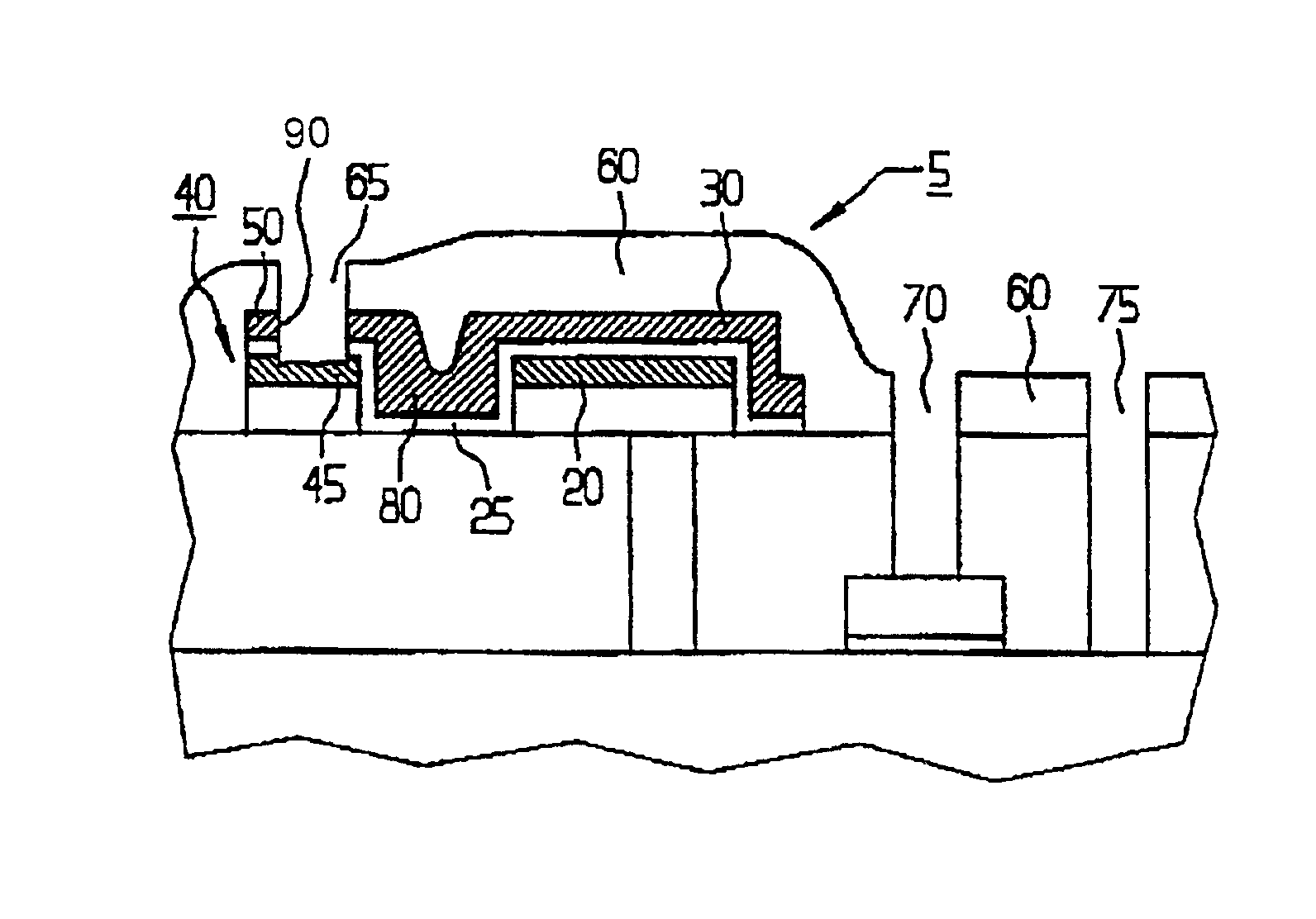
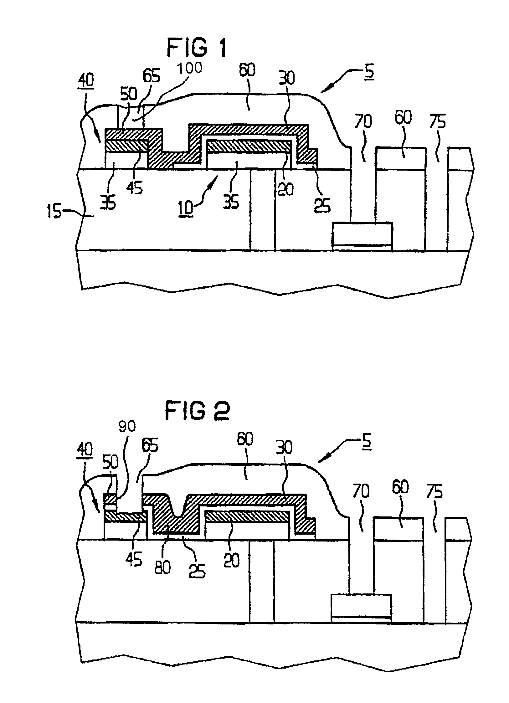
[0037]In all the figures of the drawing, sub-features and integral parts that correspond to one another bear the same reference symbol in each case. Referring now to the figures of the drawing in detail and first, particularly, to FIG. 1 thereof, there is shown a semiconductor component 5 with a memory cell 10. The memory cell 10 is disposed on an intermediate oxide 15 and is formed in layers from a first metal area 20, a dielectric layer 25 and a third metal area 30, with the two metal areas 20 and 30 representing the electrodes of the memory cell 10. The first metal area 20 is seated on a barrier layer 35 in order to prevent oxygen diffusion into the dielectric layer 25. A contact area 40 is disposed at the side adjacent to the memory cell 10, and is formed from a second metal area 45 and a fourth metal area 50, which makes direct contact with it. The third metal area 30 and the fourth metal area 50 are electrically connected to one another.

[0038]The memory cell 10 and the contact...


PUM

PropertyMeasurementUnit
dielectric constantaaaaaaaaaa
areaaaaaaaaaaa
electricallyaaaaaaaaaa

Abstract

A semiconductor component having a material-reinforced contact area formed of a metal layer is disclosed. The contact area is jointly formed by a second metal area of a first metal layer and a fourth metal area of a second metal layer which is to be contacted. A thickness of the contact area material is at least twice that of a single metal layer and thereby prevents penetrative etching when a hole is created for contacting the metal layer.

Description

CROSS-REFERENCE TO RELATED APPLICATION[0001]This is a continuation of copending International Application PCT / DE99 / 00894, filed Mar. 25, 1999, which designated the United States.BACKGROUND OF THE INVENTION[0002]Field of the Invention[0003]The invention is in the field of semiconductor technology and relates to a semiconductor component having first and second metal areas, which are both produced from a common first metal layer and are electrically insulated from one another. A second metal layer which is produced separately from the first metal layer and has a third metal area which is insulated from the first metal layer by the interposition of a dielectric layer is provided, where, together with the dielectric layer and the first metal area, it forms a memory element. A fourth metal area is provided in the second metal layer which, together with the second metal area, forms a contact area, and is used to make contact with the second metal layer. The invention also relates to a met...

Claims


Application Information

Patent Timeline
Patent Type & Authority Patents(United States)
IPC IPC(8): H01L23/52H01L23/522H01L21/768H01L21/8242H01L21/8246
CPCH01L21/76895H01L23/5226Y10S257/907H01L27/11507H01L27/10852H01L2924/0002H10B12/033H10B53/30H01L2924/00
Inventor HUBNER, HOLGERROHR, THOMAS
Owner QIMONDA
Why Eureka
Try Eureka