Mask used for exposing a porous substrate

a technology of porous substrate and mask, which is applied in the direction of circuit mask, dielectric characteristics, instruments, etc., can solve the problems of difficult to easily prepare a fine wiring structure which is three-dimensionally free in configuration, difficult to improve yield, and dimensional porous film material degradation, so as to enhance the freedom of designing a conductive circui

Inactive Publication Date: 2005-06-14
KK TOSHIBA
View PDF16 Cites 18 Cited by
  • Summary
  • Abstract
  • Description
  • Claims
  • Application Information

AI Technical Summary

Benefits of technology

[0021]Therefore, an object of the present invention is to provide a method for manufacturing a composite member comprising a substrate formed of a porous insulating body, wherein a via constituting a...

Problems solved by technology

According to the conventional method of manufacturing a wiring board however, it is very difficult to easily prepare a fine wiring structure which is three-dimensionally free in configuration.
Therefore, the formation of a via is not only very troublesome but also very difficult in improving the yield thereof.
However, it is difficult, according to the aforementioned method wherein a hole is formed in an insulating body, to form a fine via having a diameter of not more than several tens of microns at any desired region of the insulating body.
However, the method proposed by this Japanese Patent Publication is accompanied with various problems that the three-dimensional porous film material is caused to degrade due to the exposure using light having short wavelength, that the exposure beam is incapable of penetrating into the interior of the porous body as it is absorbed by the three-dimensional porous film to make it impossible to form a fine via, and that since most of the compounds to be impregnated into the three-dimensional porous film are liquid, measurements to cope with the spilling of liquid are required to be taken on the occasion of the exposure process.
However, the method proposed by this Japanese Patent Publication is accompanied with various problems that since a photosensitive composition containing a metal salt is enabled to impregnate the entire surface of a porous insulating body, it is difficult to completely remove, subsequent to the exposure process, the metal salt that has been adsorbed onto the nonexposure region, thereby permitting the generation of a phenomenon of precipitating the metal nucleus at an undesir...

Method used


Image

  • Mask used for exposing a porous substrate
  • Mask used for exposing a porous substrate
  • Mask used for exposing a porous substrate

Examples


example 1

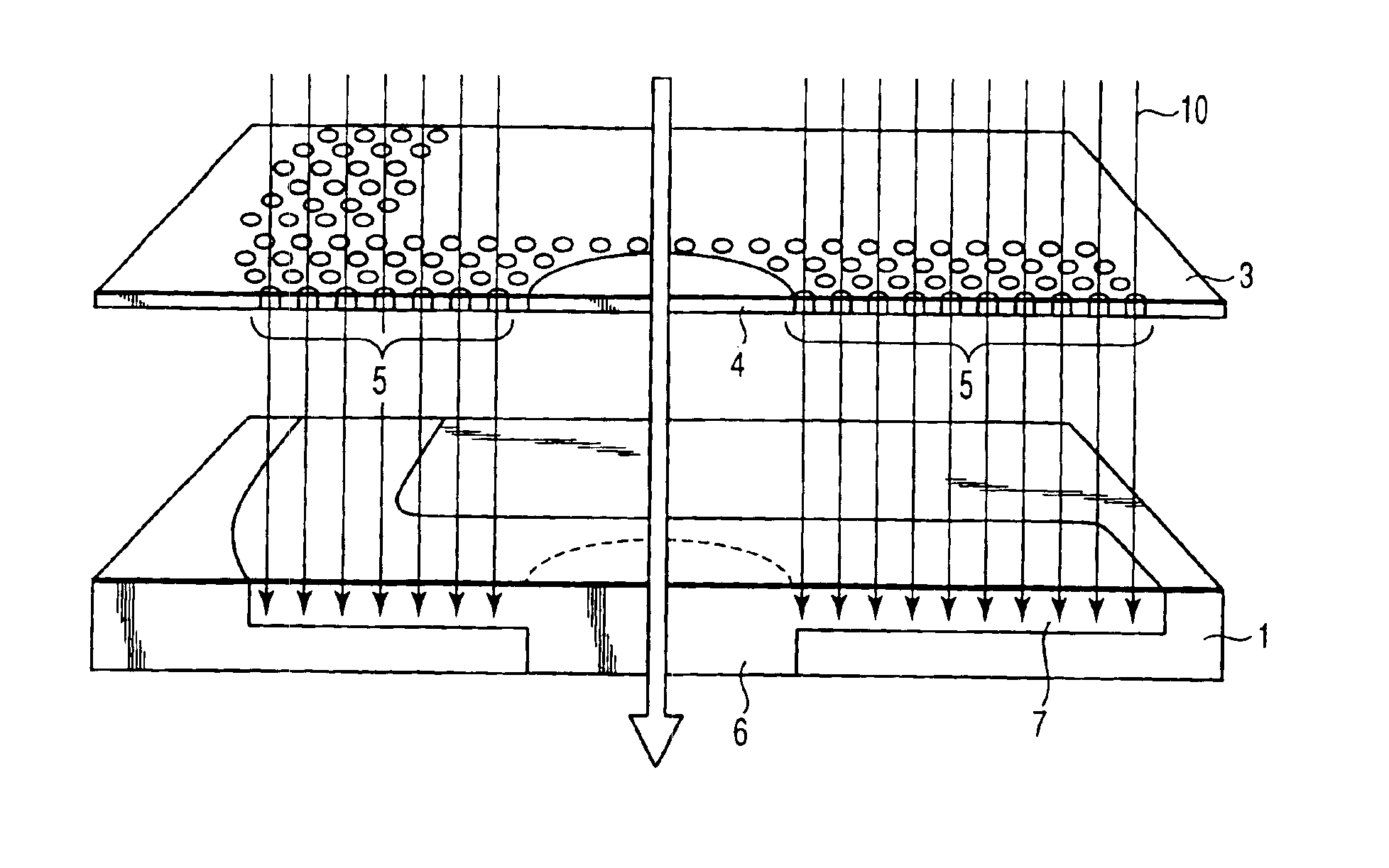
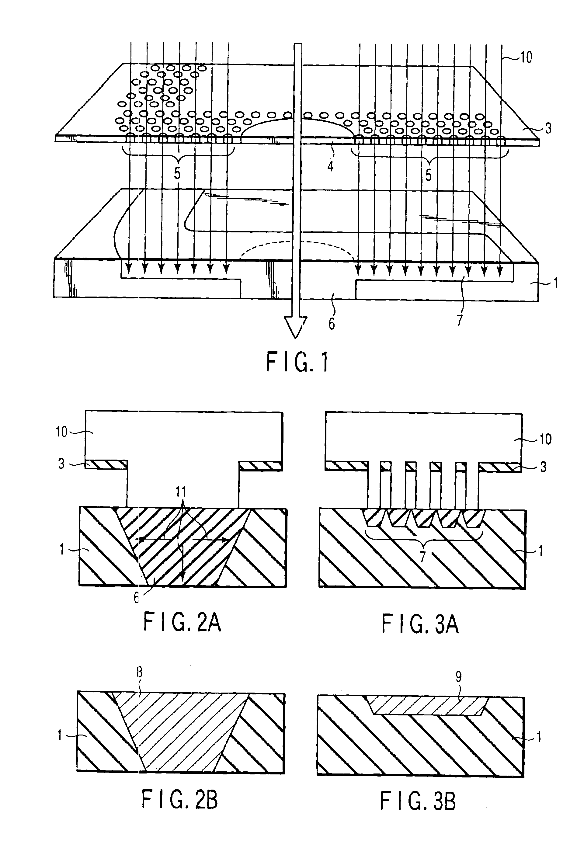
[0146]In this Example 1, the process for forming a wiring pattern in a porous insulating body by using a half-tone mask will be explained.

[0147]As a porous substrate, a PTFE porous sheet (the diameter of void: 500 nm, and the film thickness: 58 μm) was prepared. In the meantime, naphthoquinone diazide-containing phenol resin (the content of naphthoquinone diazide: 33 equivalent mol. %) was dissolved in acetone to prepare a 1 wt. % acetone solution as a photo-sensitizer, which was then coated on the entire surface of the porous sheet by a dipping method. As a result, not only the interior of the holes of the porous sheet but also the surface of the inner voids was covered with a photo-sensitizer.

[0148]Then, the resultant sheet was irradiated through a mask with a beam having a wavelength of 436 nm by using CANON PLA501 to generate an ion-exchange group at the irradiated or exposed portion. The mask employed in this case was a half-tone mask, the schematical construction of which bein...

example 2

[0157]In this Example 2, the process for forming a wiring and a via in a porous insulating body by using a mask having a fine pattern will be explained.

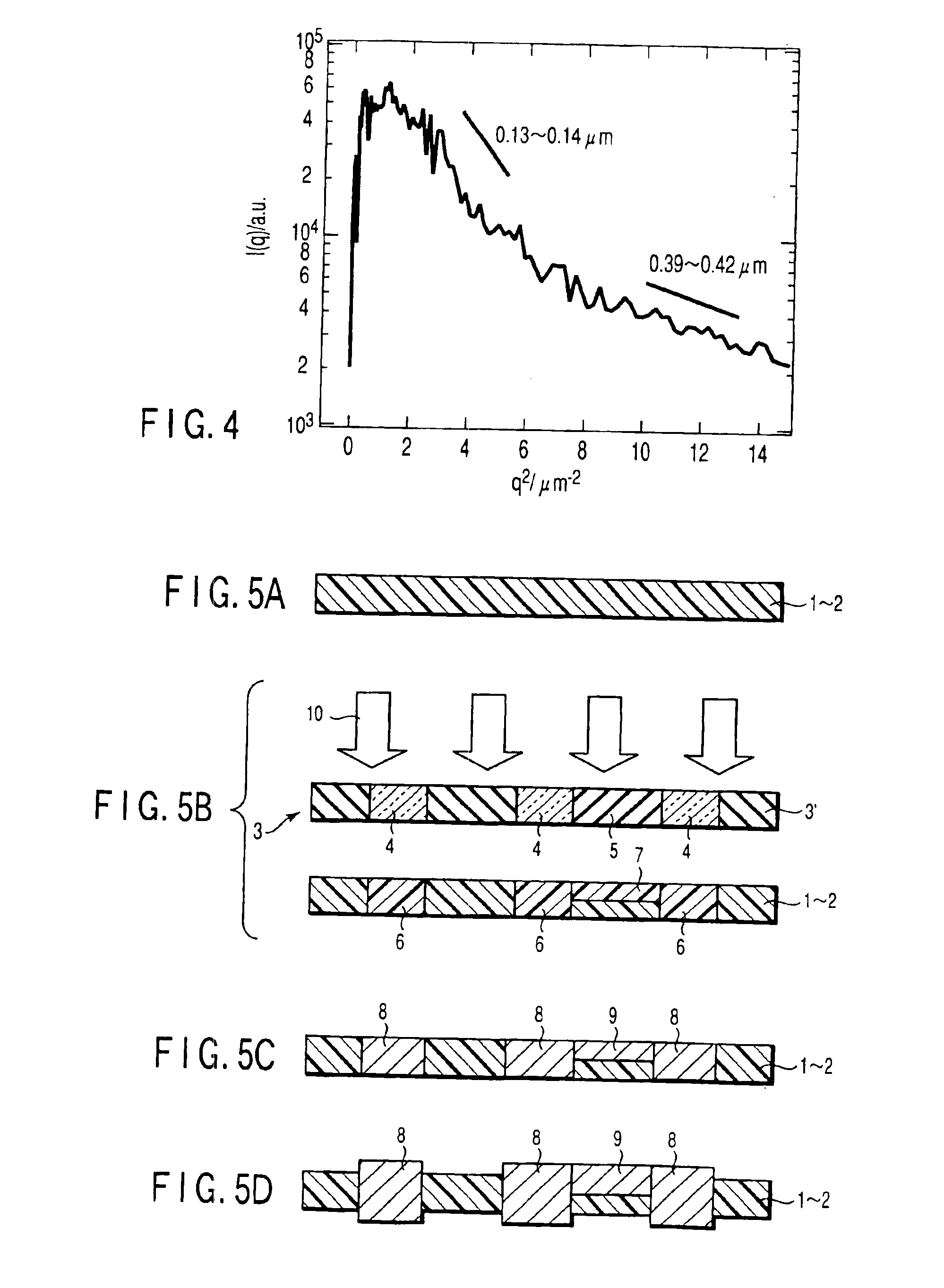
[0158]First of all, by the same procedures as employed in the aforementioned Example 1, a sample was prepared by coating a photo-sensitizer on the surface of an insulating body. Then, the sample was irradiated, via a mask and by using CANON PLA 501, with a beam having a wavelength of 436 nm, thereby enabling an ion-exchange group to be generated at the exposure portion. When the size of voids of the insulating body employed in this example was defined in terms of a radius of gyration as in the case of Example 1, it was 0.89 to 0.96 time as large as the wavelength of the exposure beam.

[0159]The mask employed in this example was provided at the wiring portion thereof with a fine pattern, a schematic view of which is shown in FIG. 7.

[0160]As shown in FIG. 7, the mask 30 was provided with a beam-transmitting region 31 for photo-sensitizi...

example 3

[0186]In this Example 3, the process for simultaneously forming a couple of wiring patterns on the opposite surfaces of substrate and a via in the substrate will be explained.

[0187]As a porous substrate, a PTFE porous sheet (the diameter of void: 600 nm, and the film thickness: 102 μm) was employed. In the meantime, a sample was prepared by coating the substrate with a photo-sensitizer by the same method as described in Example 1 except that this insulating film was employed as the porous substrate.

[0188]As for the mask to be employed for performing the exposure from the opposite surfaces of the sample, a mask comprising a top sheet and a bottom sheet each provided, at the wiring portions thereof, with a fine pattern was prepared.

[0189]The schematic structure of the mask employed herein is shown in FIG. 9.

[0190]As shown in FIG. 9, the mask was constituted by a combination of a pear of masks, i.e. a top surface exposure mask 40a and a bottom surface exposure mask 40b. These masks 40a...


PUM

PropertyMeasurementUnit
Lengthaaaaaaaaaa
Lengthaaaaaaaaaa
Fractionaaaaaaaaaa

Abstract

A mask used for exposing a porous substrate to form a first region and a second region, the first region being filled with a conductive material piercing through the entire thickness of the porous substrate to constitute an interfacial conductive portion, the second region being filled with a conductive material not piercing the entire thickness of the porous substrate to constitute a non-interfacial conductive portion. The mask includes a first light-transmitting region for exposing the first region, and a second light-transmitting region for exposing the second region, said second light-transmitting region including an aggregation of fine patterns of which an average aperture ratio is not more than 50% of an average aperture ratio of the first light-transmitting region and a size of said fine patterns of the second light-transmitting region being in the range of 0.1 μm to 10 μm.

Description

CROSS-REFERENCE TO RELATED APPLICATIONS[0001]This application is based upon and claims the benefit of priority under 37 CFR § 19 from the prior Japanese Patent Applications No. 2001-170018, filed Jun. 5, 2001; and No. 2001-295461, filed Sep. 27, 2001, and under 37 CFR §120 which is a division of U.S. Application Ser. No. 10 / 161,707 filed Jun. 5, 2002, which has now issued as U.S. Pat. No. 6,649,516, entire continents of which are incorporated herein by reference.BACKGROUND OF THE INVENTION[0002]1. Field of the Invention[0003]This invention relates to a method for manufacturing a composite member comprising an insulating body which is provided with a conductive region such as a wiring, the composite member being designed to be employed as a wiring board in various technical fields such as electrics, electronics and telecommunications.[0004]2. Description of the Related Art[0005]In recent years, there has been a prominent advance with regard to the integration and miniaturization of v...

Claims


Application Information

Patent Timeline
IPC IPC(8): H05K3/00H05K3/10H05K3/42H05K3/18H05K1/03
CPCH05K3/0082H05K3/107H05K3/185H05K3/422H05K1/034H05K3/0002Y10T428/12042H05K2201/0116H05K2201/015H05K2203/056H05K2203/107H05K2203/1147G03F1/50G03F1/86
Inventor ASAKAWA, KOJIHOTTA, YASUYUKIMATAKE, SHIGERUHIRAOKA, TOSHIRO
Owner KK TOSHIBA
Why Eureka
Try Eureka