Polymide-to-substrate adhesion promotion in HDI

a technology of polymide and substrate, applied in the direction of layered products, basic electric elements, cable/conductor manufacturing, etc., can solve the problems of inability to soften the spie by heating, copper is not the best material for electrical contacts, and adhesion often fails

Inactive Publication Date: 2005-06-21
LOCKHEED MARTIN CORP
View PDF7 Cites 25 Cited by
  • Summary
  • Abstract
  • Description
  • Claims
  • Application Information

AI Technical Summary

Benefits of technology

[0011]In particular modes of the method according to the invention, the step of etching the one of the copper-, titanium-, and copper-and titanium-containing portions of the substrate with a liquid etchant includes the step of (a) etching with cupric chloride if the portions contain copper, (b) etching with HF if the portions contain titanium, and (c) etching with both cupric chloride and HF if the portions contain both copper and titanium, with the step of etching with HF preceding the step of etching with cupric chloride. It has been found that good adhesion promoters are VM651, manufactured by HD Microsystems of Parlin, N.J., and T2902, manufactured by United Chemical Technologies. In one variant of the method, the step of applying SPIE varnish to the cured adhesion promoter includes the step of applying SPIE varnish to a thickness of 4 micrometers. In another version, the step of curing the SPIE varnish includes the steps of curing the SPIE varnish for a period of time at a first temperature, and then curing the SPIE varnish for a second period of time at a second temperature, greater than the first temperature. In one avatar, the first and second periods of time each have a duration of about 1 hour. When these durations are used, the curing for a first period of time is performed at about 100° Celsius, and the curing for the second period of time is performed at a temperature of about 190° Celsius. The step of curing the adhesion promoter to thereby produce cured adhesion promoter may be performed for 15 minutes at 100° C. Similarly, the step of curing the adhesive surface to form a cured adhesive surface may be performed for 15 minutes at 100° C. The cured SPIE varnish may be cooled between the steps of curing the SPIE varni...

Problems solved by technology

Once set, the SPIE cannot be softened by heating.
The integration of such modules presents some problems, in that the manufacturers of the components are accustomed to using copper as the main conductive material, and to making the electrical contacts from copper.
Copper is not the best material for electrical contacts in an HDI context, because it oxidizes readily, especially in the presence of high temperatures.
Even if they initially appear to adhere, the adhesion often fails in the presence of heat or moisture.
Thus, a copper su...

Method used


Image

  • Polymide-to-substrate adhesion promotion in HDI
  • Polymide-to-substrate adhesion promotion in HDI
  • Polymide-to-substrate adhesion promotion in HDI

Examples


Embodiment Construction

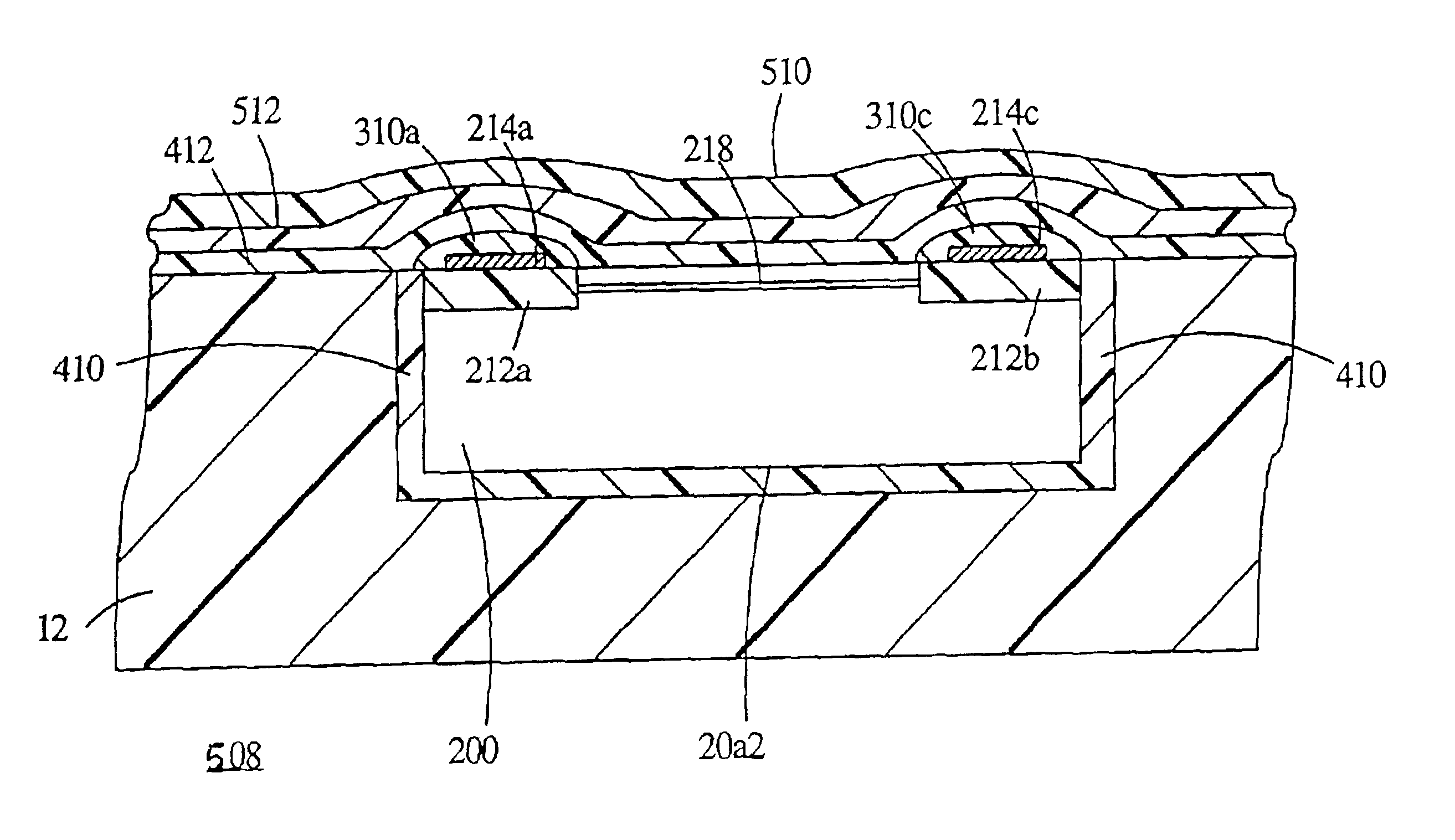
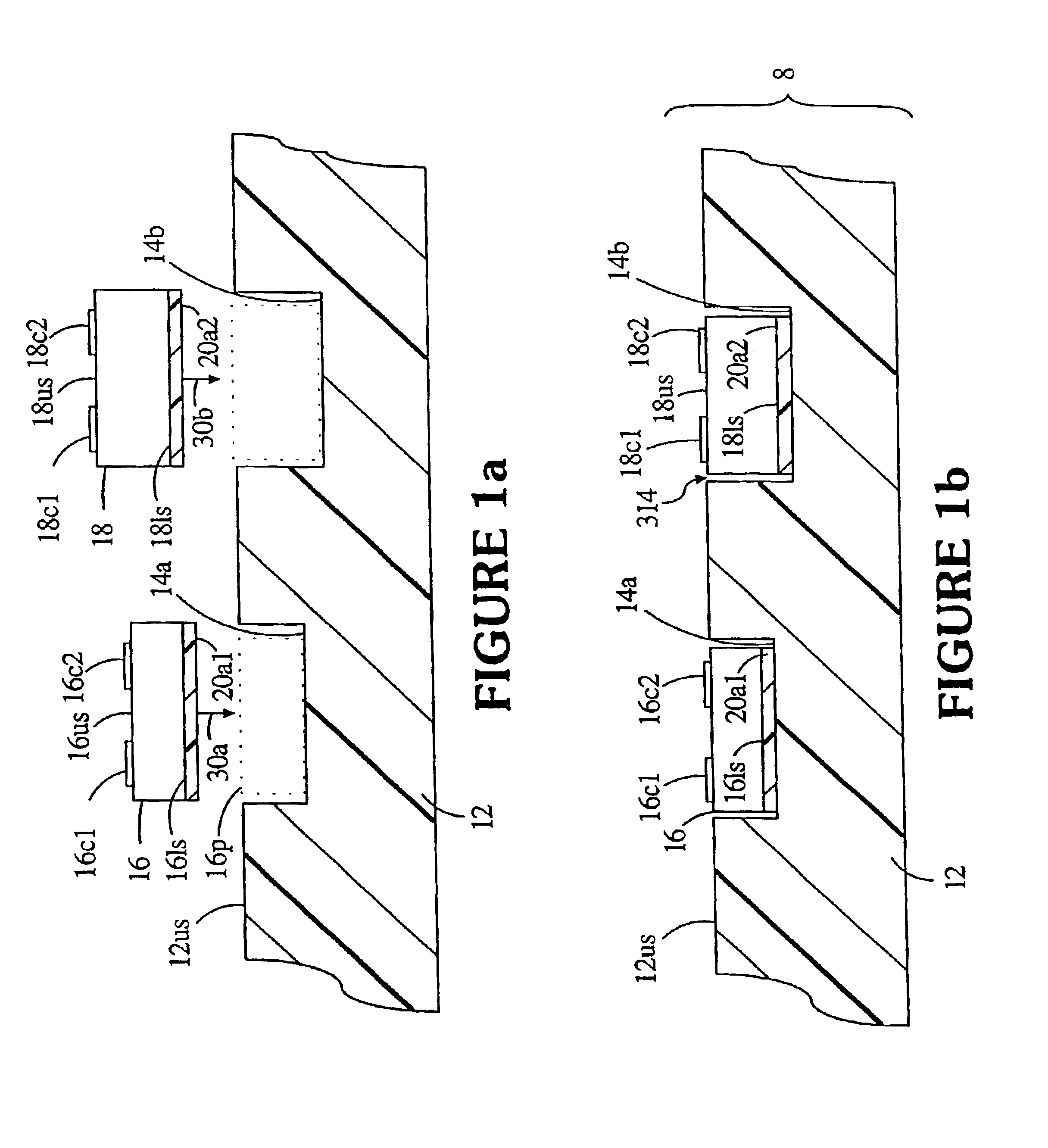
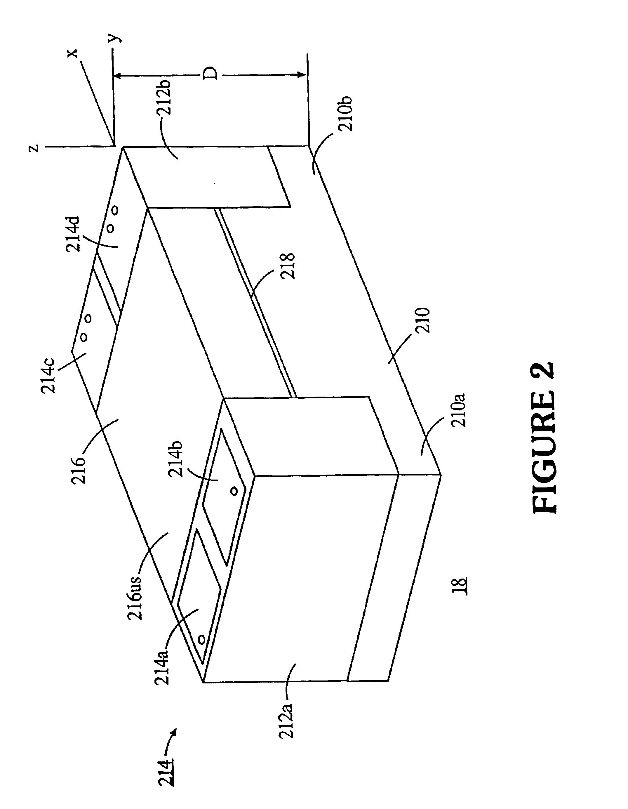
[0030]In FIG. 1a, a high-density-interconnect (HDI) dielectric substrate 12 defines a planar upper surface 12us, and first and second wells 14a and 14b depressed below surface 12us. Instead of wells, through apertures could be used. As illustrated, a first component 16 defines an upper surface 16us and a lower surface 16ls. Upper surface 16us of component 16 bears a plurality of electrical connections, two of which are illustrated as 16c1 and 16c2. The phantom lines 16p illustrate the location of component 16 when mounted in well 14a. When component 16 is mounted within well 14a, the plane of its upper surface 16us is substantially coincident with the plane of upper surface 12us of dielectric substrate 12. Also in FIG. 1a, a second component 18 defines an upper surface 18us and a lower surface 18ls. Upper surface 18us of component 18 bears a plurality of electrical connections, two of which are illustrated as 18cl and 18c2. The phantom lines 18p illustrate the location of component ...


PUM

PropertyMeasurementUnit
Temperatureaaaaaaaaaa
Timeaaaaaaaaaa
Thicknessaaaaaaaaaa

Abstract

Methods for adhering polyimide dielectric materials to copper-, titanium-, aluminum-, or copper-and-titanium-containing portions of a substrate are described. The methods include the steps of applying adhesion promoter to a clean surface of the substrate, and curing the adhesion promoter. SPIE varnish is applied over the cured adhesion promoter, and is itself cured. A further layer of adhesion promoter is applied over the cured SPIE varnish, and is cured. The polyimide dielectric material is then laminated to the adhesion promoter. Cleaning of the copper-containing substrate portions is performed by etching with etchant including cupric chloride, cleaning of the titanium-containing substrate portions is performed with etchant including HF, and cleaning of copper- and titanium-containing portions is performed by HF etching followed by cupric chloride etching. Aluminum-containing portions of the substrate are not etched.

Description

[0001]This application claims priority from Provisional application Ser. No. 60 / 333,204 filed Nov. 6, 2001.FIELD OF THE INVENTION[0002]This invention relates to methods for making reliable connection of polyimide to copper-, titanium-, andor aluminum-containing substrate materials.BACKGROUND OF THE INVENTION[0003]High density interconnect assemblages such as those described in U.S. Pat. No. 4,783,695, issued Nov. 8, 1988 in the name of Eichelberger et al., and in numerous other patents, are finding increased usage. In the typical HDI assemblage, a dielectric substrate such as alumina has a planar surface and one or more wells or depressions. Each well or depression extends below the planar surface by the dimension of a component which is to become part of the HDI assemblage. The component is typically an integrated circuit, having its electrical connections or contacts on an upper surface. These contacts or connections are preferably made from titanium-coated copper-containing metal...

Claims


Application Information

Patent Timeline
IPC IPC(8): B32B9/04H01L21/60H01L23/538H01L25/16
CPCH01L23/5389H01L24/24H01L24/29H01L24/76H01L24/82H01L2924/00013H01L2924/0665H01L2924/01072H01L2924/01033H01L2924/01006H01L2224/29298H01L2224/29H01L2924/00011H01L2924/3025H01L2924/19042H01L2924/15165H01L2924/15153H01L2924/14H01L2924/01075H01L2924/0105H01L2924/01046H01L2924/01029H01L25/16H01L2224/2402H01L2224/24227H01L2224/2919H01L2224/32225H01L2224/82039H01L2224/83191H01L2224/83855H01L2224/92244H01L2924/01005H01L2924/01013H01L2924/01018H01L2924/00H01L2224/29099H01L2224/29199H01L2224/29299H01L2224/2929H01L2224/73267H01L2224/04105
Inventor FOUST, DONALD FRANKLINNEALON, WILLIAM FRANCISDAVIES, JR., ROBERT G.CREPEAU, CHARLES E.
Owner LOCKHEED MARTIN CORP
Why Eureka
Try Eureka