ATR-FTIR metal surface cleanliness monitoring

Inactive Publication Date: 2005-06-21
TAIWAN SEMICON MFG CO LTD
View PDF9 Cites 8 Cited by
  • Summary
  • Abstract
  • Description
  • Claims
  • Application Information

AI Technical Summary

Benefits of technology

[0011]The invention relates to attenuated total reflectance (ATR)-Fourier transform infrared (FTIR) metal surface cleanliness monitoring. A metal surface of a semiconductor die is impinged with an infrared (IR) beam, such as can be accomplished by using an ATR technique. The IR beam as reflected by the metal surface is measured. For instance, an interferogram of the reflected IR beam may be measured. A Fourier transform of the interferogram may also be performed, in accordance with an FTIR technique. To determine whether the metal surface is contaminated, the IR beam as reflected is compared to a reference sample. For example, the Fourier transform of the interferogram may be compared to the reference sample. If there is deviation by more than a threshold, the metal surface may be conclud

Problems solved by technology

Furthermore, the process is relatively fast, ensuring a high throughput, and is highly sensitive.

Method used


Image

  • ATR-FTIR metal surface cleanliness monitoring
  • ATR-FTIR metal surface cleanliness monitoring
  • ATR-FTIR metal surface cleanliness monitoring

Examples


Embodiment Construction

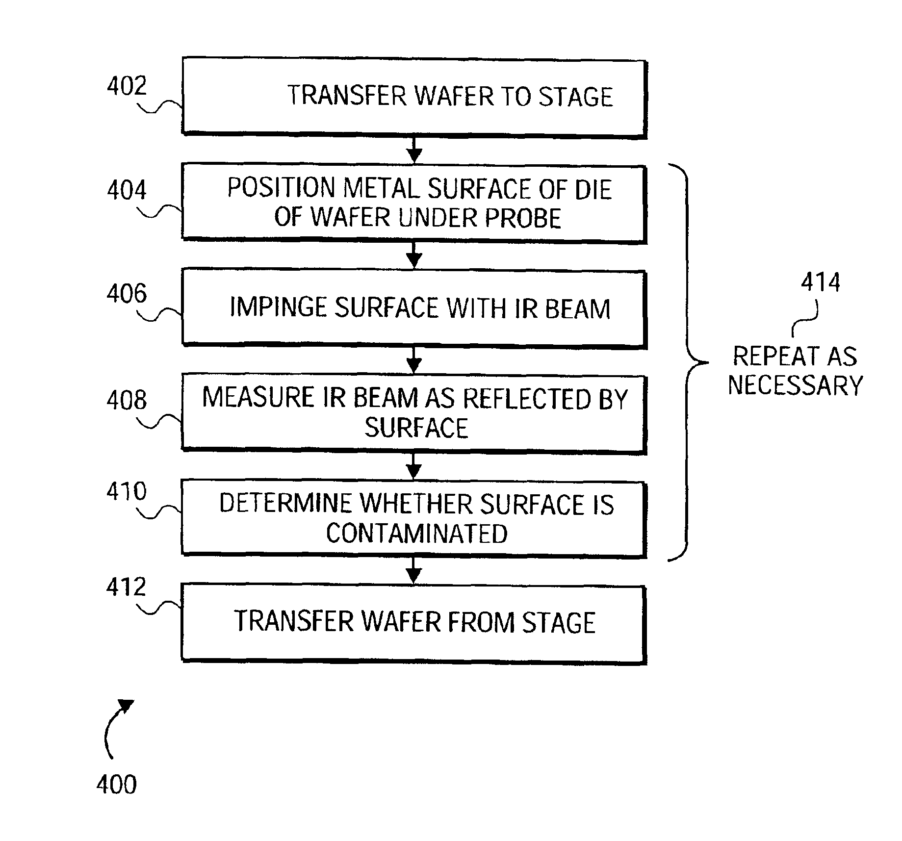
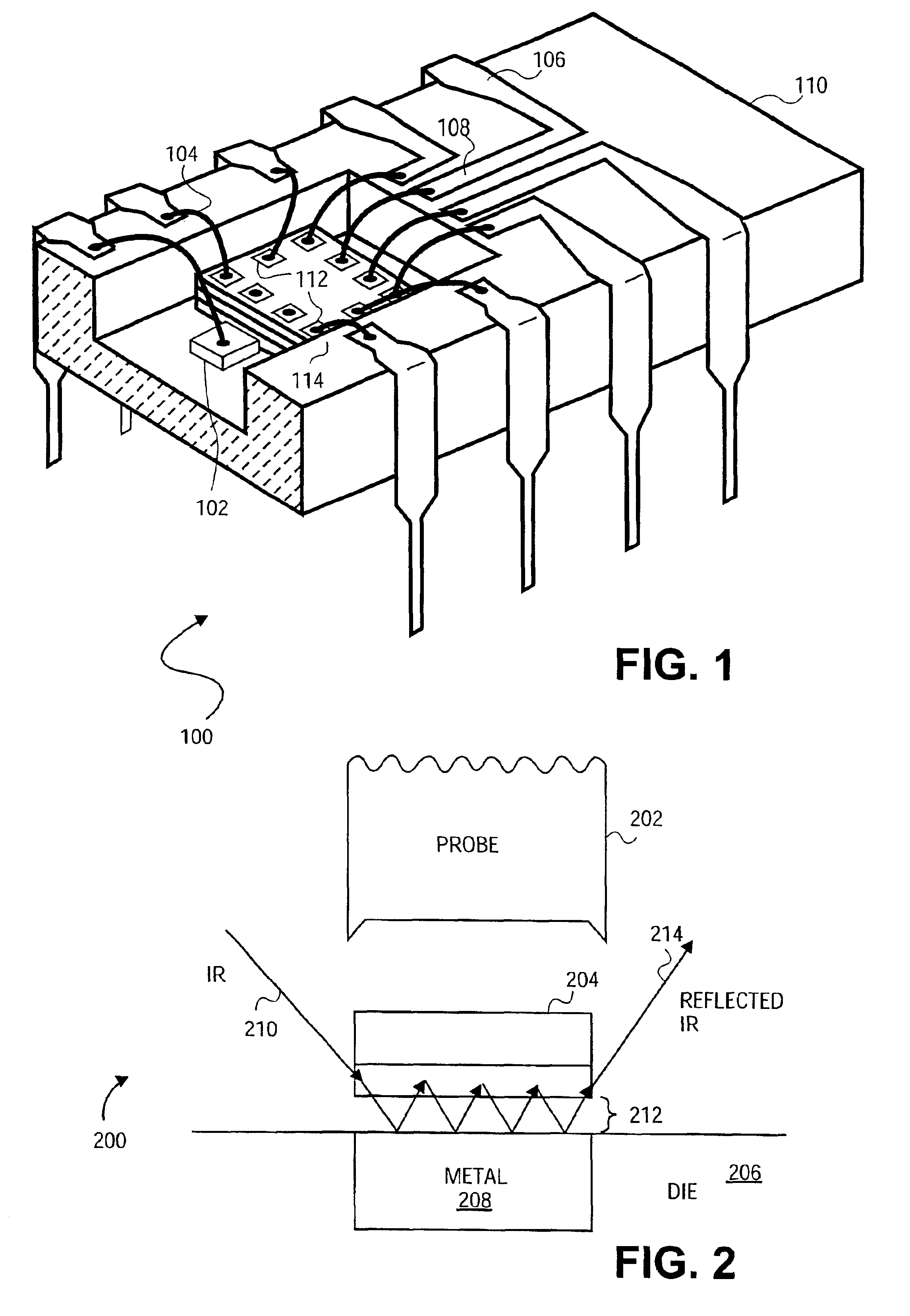
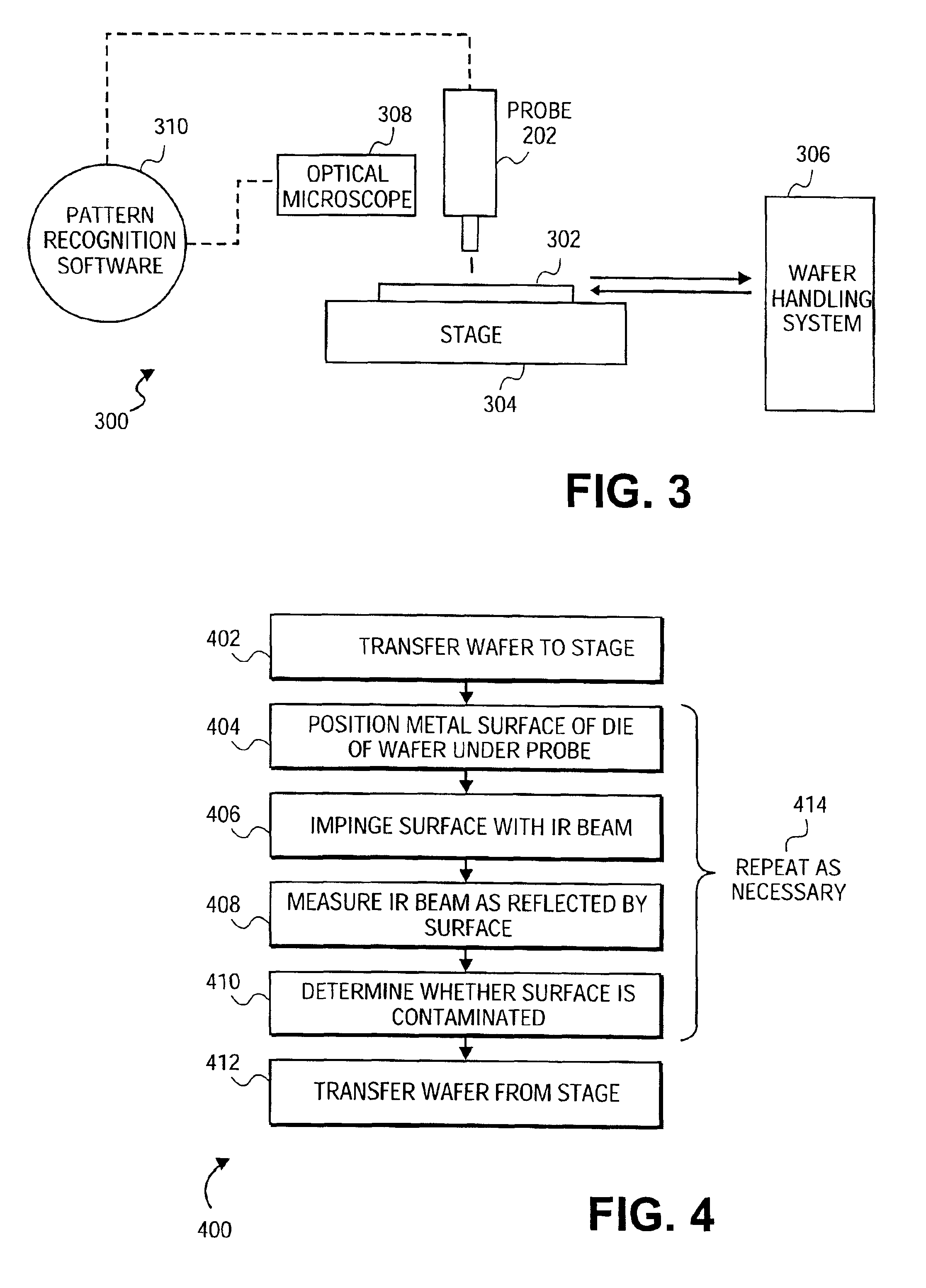
[0017]In the following detailed description of exemplary embodiments of the invention, reference is made to the accompanying drawings that form a part hereof, and in which is shown by way of illustration specific exemplary embodiments in which the invention may be practiced. These embodiments are described in sufficient detail to enable those skilled in the art to practice the invention. Other embodiments may be utilized, and logical, mechanical, and other changes may be made without departing from the spirit or scope of the present invention. The following detailed description is, therefore, not to be taken in a limiting sense, and the scope of the present invention is defined only by the appended claims. For instance, whereas the invention is substantially described in relation to a bonding pad, it is applicable to other metal surfaces of semiconductor dies of semiconductor wafers as well, such as metal trenches, and so on.

[0018]FIG. 2 shows a system 200 according to an embodiment...


PUM


Abstract

Attenuated total reflectance (ATR)-Fourier transform infrared (FTIR) metal surface cleanliness monitoring is disclosed. A metal surface of a semiconductor die is impinged with an infrared (IR) beam, such as can be accomplished by using an ATR technique. The IR beam as reflected by the metal surface is measured. For instance, an interferogram of the reflected IR beam may be measured. A Fourier transform of the interferogram may also be performed, in accordance with an FTIR technique. To determine whether the metal surface is contaminated, the IR beam as reflected is compared to a reference sample. For example, the Fourier transform of the interferogram may be compared to the reference sample. If there is deviation by more than a threshold, the metal surface may be concluded as being contaminated.

Description

FIELD OF THE INVENTION[0001]This invention relates generally to metal surfaces of semiconductor devices, such as bonding pads, and more particularly to monitoring the cleanliness of such metal surfaces.BACKGROUND OF THE INVENTION[0002]Once semiconductor devices on semiconductor wafers have been fabricated, they must be packaged in order to actually be used. The individual dies on the wafers are separated from one another, and then are typically put in a protective package. They may also be mounted onto the surface of a ceramic substrate as part of a hybrid circuit, put into a large package with other chips as part of a multi-chip module (MCM), or be connected directly on board a printed circuit or chip-on-board (COB). However, packaging the wafers individually into protective packages is still the most common back-end process.[0003]FIG. 1 shows an example of a partially exposed packaged chip 100. The packaged chip 100 includes a die-attachment area 102. This is typically located in ...

Claims


Application Information

Patent Timeline
IPC IPC(8): G01N21/31G01N21/35G01N21/55
CPCG01N21/35G01N21/552G01N21/3563G01N2021/3595G01N21/94
Inventor LI, LAIN-JONGJANG, SYUN-MINGKO, CHUNG-CHI
Owner TAIWAN SEMICON MFG CO LTD
Why Eureka
Try Eureka