Printed circuit board with embedded capacitors therein, and process for manufacturing the same

Inactive Publication Date: 2005-06-28
SAMSUNG ELECTRO MECHANICS CO LTD
View PDF9 Cites 70 Cited by
  • Summary
  • Abstract
  • Description
  • Claims
  • Application Information

AI Technical Summary

Benefits of technology

[0053]Therefore, the present invention has been made in view of the above problems, and it is an object of the present invention to provide a printed circuit board with embedded capacitors therein and a process f

Problems solved by technology

Since a market for the printed circuit boards with embedded capacitors therein is small, the standardization of these techniques is not yet achieved and trials to develop commercially available processes are still ongoing.
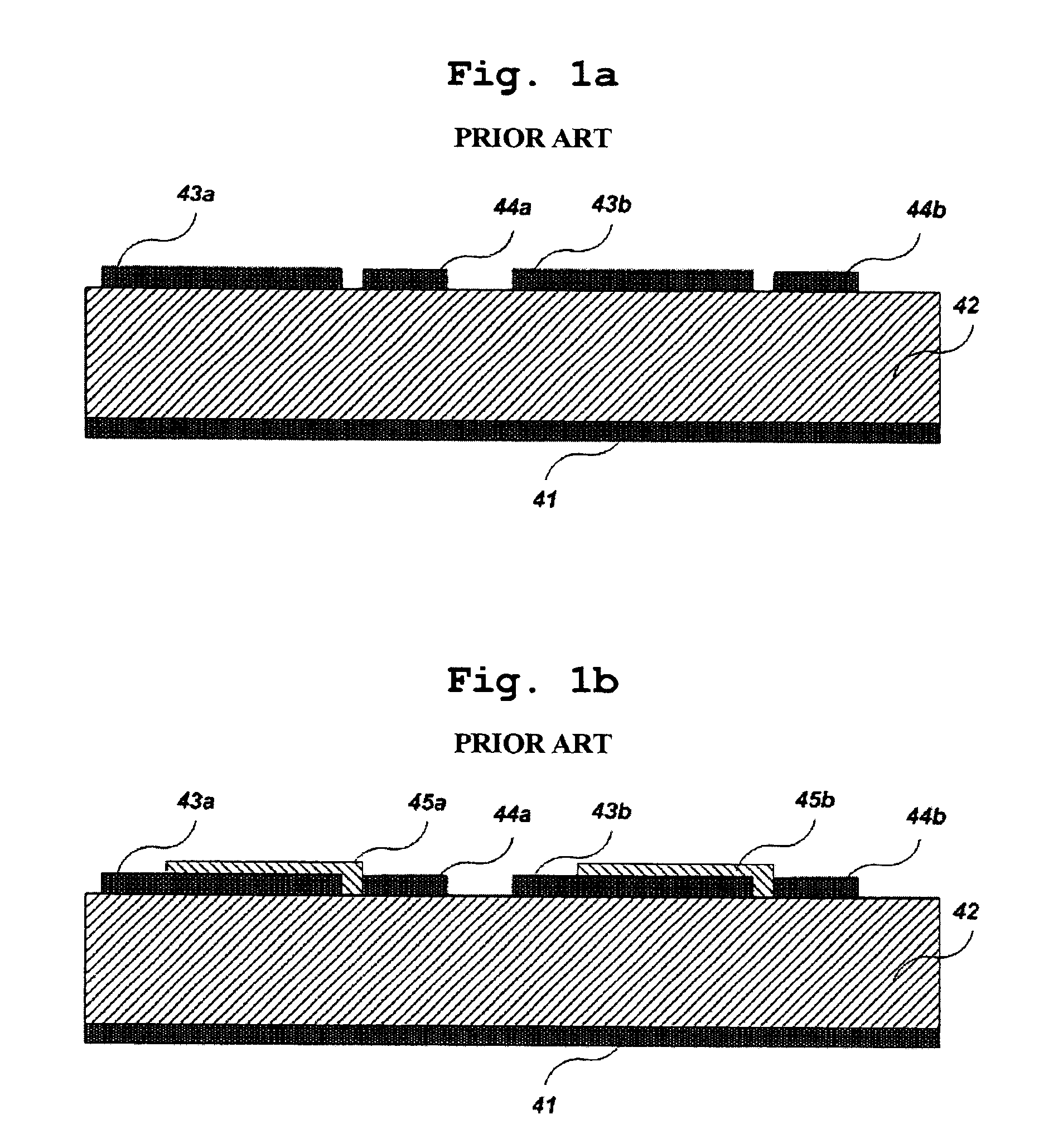
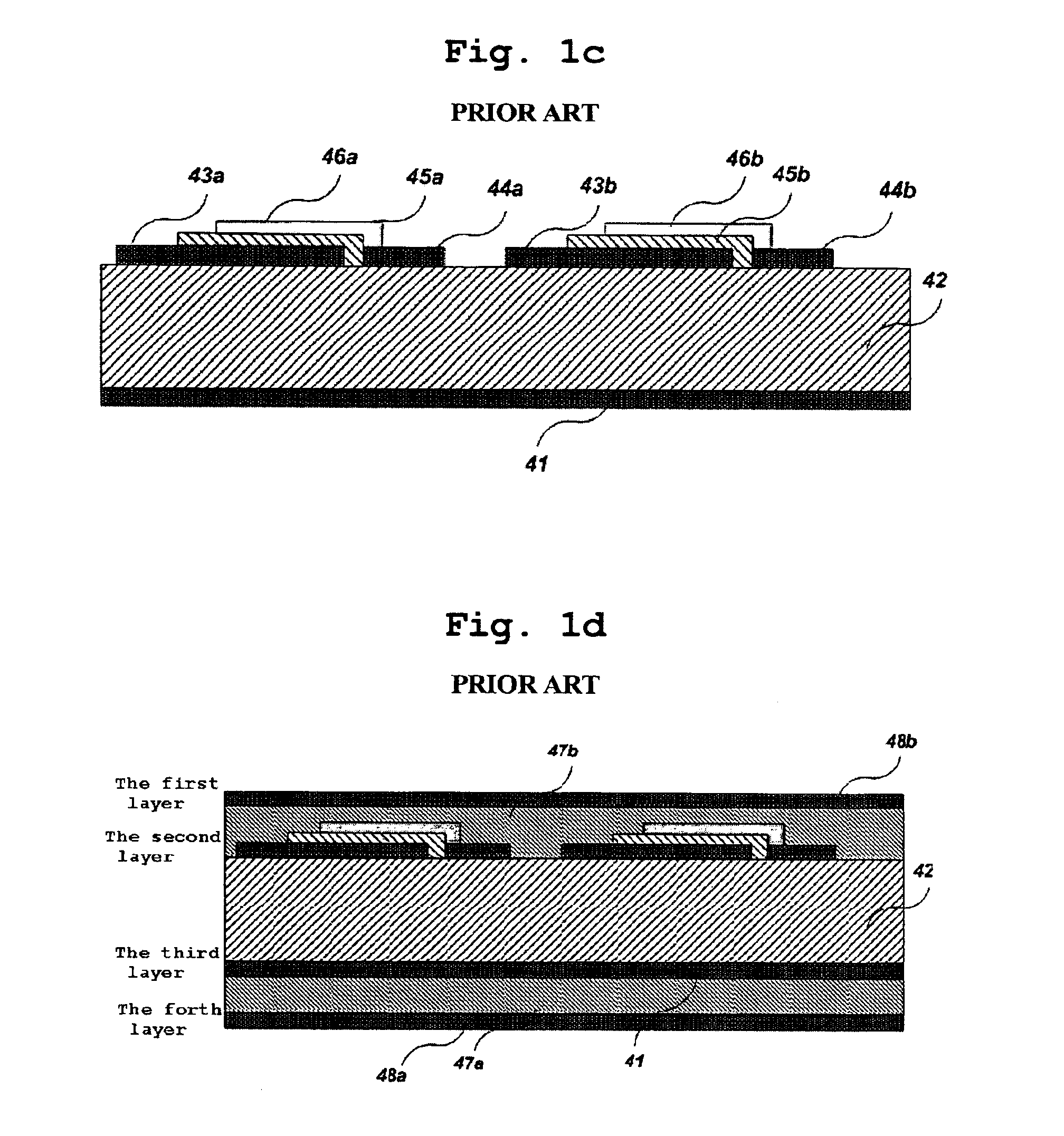
One of the problems concerning the first technique of the conventional techniques discussed above is the occurrence of cracks of the capacitor pastes 45a and 45b at ends of the positive (+) electrodes 46a and 46b.
The occurrence of cracks (C) results from the thickness of the copper foils for negative (−) electrodes.
Since the thickness of the printed capacitors is about 10 μm, cracks occur at ends of the copper foils for negative (−) electrodes.
The cracks also cause problems that when the copper pastes 45a and 45b connected to the copper foils 44a and 44b for positive (+) electrodes are printed, an interlayer short between the negative (−) electrodes and the positive (+) electrodes is poor.
In addition, the second problem concerning the first technique of the conventional techniques discussed above is non-uniform insulation distance between a first layer and a second layer shown in FIG. 1e.
The difference in the insulation distances leads to poor impedance of signal circuits in the first layer and the second layer.
Furthermore, the third problem concerning the first technique of the conventional techniques discussed above is the presence of impurities occurring during printing and drying of the capacitor pastes 45a and 45b and copper pastes 46a and 46b.
At this time, impurities occur during the printing.
The first problem conc

Method used


Image

  • Printed circuit board with embedded capacitors therein, and process for manufacturing the same
  • Printed circuit board with embedded capacitors therein, and process for manufacturing the same
  • Printed circuit board with embedded capacitors therein, and process for manufacturing the same

Examples


Example

[0090]Hereinafter, a printed circuit board with embedded capacitors therein and a process for manufacturing the printed circuit board according to the embodiments of the present invention will be explained in more detail with reference to the accompanying drawings.

[0091]FIG. 6 is a cross-sectional view showing a printed circuit board with embedded capacitors therein according to the present invention, the capacitors being formed by the application of a photosensitive insulating resin and a polymer capacitor paste

[0092]Referring to FIG. 6, capacitors are formed by applying a photosensitive insulating resin 103 to copper foils formed on a copper clad FR-4 101, applying capacitor pastes 104a to 104d to etched regions of the photosensitive insulating resin 103, and forming top electrodes 105a to 105d on surfaces of the photosensitive insulating resin. The printed circuit board with embedded capacitors therein according to the present invention is commonly composed of six layers wherein ...


PUM

PropertyMeasurementUnit
Temperatureaaaaaaaaaa
Lengthaaaaaaaaaa
Thicknessaaaaaaaaaa

Abstract

Disclosed herein are a printed circuit board with embedded capacitors therein and a process for manufacturing the printed circuit board. The embedded capacitors are formed by applying a photosensitive insulating resin to a printed circuit board inner layer, and applying a high dielectric polymer capacitor paste thereto. The process for manufacturing a printed circuit board with embedded capacitors therein comprises the steps of: i) laminating photoresist dry films to a copper clad FR-4, exposing to light and developing the dry films, and etching copper foils of the copper clad FR-4 to form bottom electrodes for forming capacitors; ii) applying a photosensitive insulating resin to the surfaces of the bottom electrodes, and exposing to light and developing to etch the photosensitive insulating resin; iii) applying a capacitor paste to the etched regions and curing the capacitor paste; iv) plating the upper regions of the cured capacitor paste and the photosensitive insulating resin using an electroless copper plating process to form copper foil layers for top electrodes; v) laminating photosensitive dry films to the copper foil layers for top electrodes, and exposing to light and developing the photosensitive dry films to etch regions of the dry films except for the copper foil layers where the top electrodes are to be formed; and vi) etching the regions of the dry films except for the copper foil layers where the top electrodes are to be formed, and the dry films formed on the top electrodes are removed so that the capacitor paste is discretely positioned between the top electrodes and the bottom electrodes to form discrete capacitors.

Description

BACKGROUND OF THE INVENTION[0001]1. Field of the Invention[0002]The present invention relates to a printed circuit board with embedded capacitors therein, and a process for manufacturing the printed circuit board. More particularly, the present invention relates to a printed circuit board with embedded capacitors therein in which the embedded capacitors are formed by applying a photosensitive insulating resin to a printed circuit board (PCB) inner layer and applying a high dielectric polymer capacitor paste thereto, and a process for manufacturing the printed circuit board.[0003]2. Description of the Related Art[0004]Common discrete chip resistors or discrete chip capacitors have been mounted on the surfaces of conventional printed circuit boards (PCBs). Recently, printed circuit boards with embedded passive devices such as resistors, capacitors, etc. therein are developed.[0005]Such printed circuit boards with embedded passive devices therein are manufactured by a process comprisin...

Claims


Application Information

Patent Timeline
IPC IPC(8): H05K1/16H05K3/00H05K3/46H05K3/42
CPCH05K1/162H05K3/0023H05K3/429H05K3/4652H05K3/4661Y10T29/49155H05K2201/0209H05K2203/0568Y10T29/49117Y10T29/4913H05K2201/0187H05K3/46
Inventor LEE, SEOK-KYUKANG, JANG-KYUJIN, HYUN-JUMIN, BYOUNG-YOUL
Owner SAMSUNG ELECTRO MECHANICS CO LTD
Why Eureka
Try Eureka