Semiconductor integrated circuit device operating with low power consumption

a technology of integrated circuit device and low power consumption, which is applied in the direction of logic circuit coupling/interface arrangement, pulse technique, instruments, etc., can solve the problems of inability to achieve the reduction of operation power supply voltage, difficulty in reducing the absolute value of threshold voltage, and increase of leakage current, etc., to achieve high integration and suppress current consumption

Inactive Publication Date: 2005-06-28
RENESAS ELECTRONICS CORP
View PDF23 Cites 8 Cited by
  • Summary
  • Abstract
  • Description
  • Claims
  • Application Information

AI Technical Summary

Benefits of technology

[0031]An object of the present invention is to provide a semiconductor device, which can suffic

Problems solved by technology

However, it is difficult to reduce the absolute value of the threshold voltage according to the scaling rule.
Therefore, such a problem occurs that the off-leak current increases to increase the standby current in a standby cycle during which MIS transistors are off.
In this case, however, reduction of the operation power supply voltage cannot achieve an intended effect, and fast operation cannot be ensured.
In the case where the thickness of gate insulating film is reduced in accordance with lowering of the operation power supply voltage and is reduced to about 3 nm in accordance with the condition that the power supply voltage is 1.5 V or lower, for example, a tunnel current flows through the gate insula

Method used


Image

  • Semiconductor integrated circuit device operating with low power consumption
  • Semiconductor integrated circuit device operating with low power consumption
  • Semiconductor integrated circuit device operating with low power consumption

Examples


first embodiment

[0156][First Embodiment]

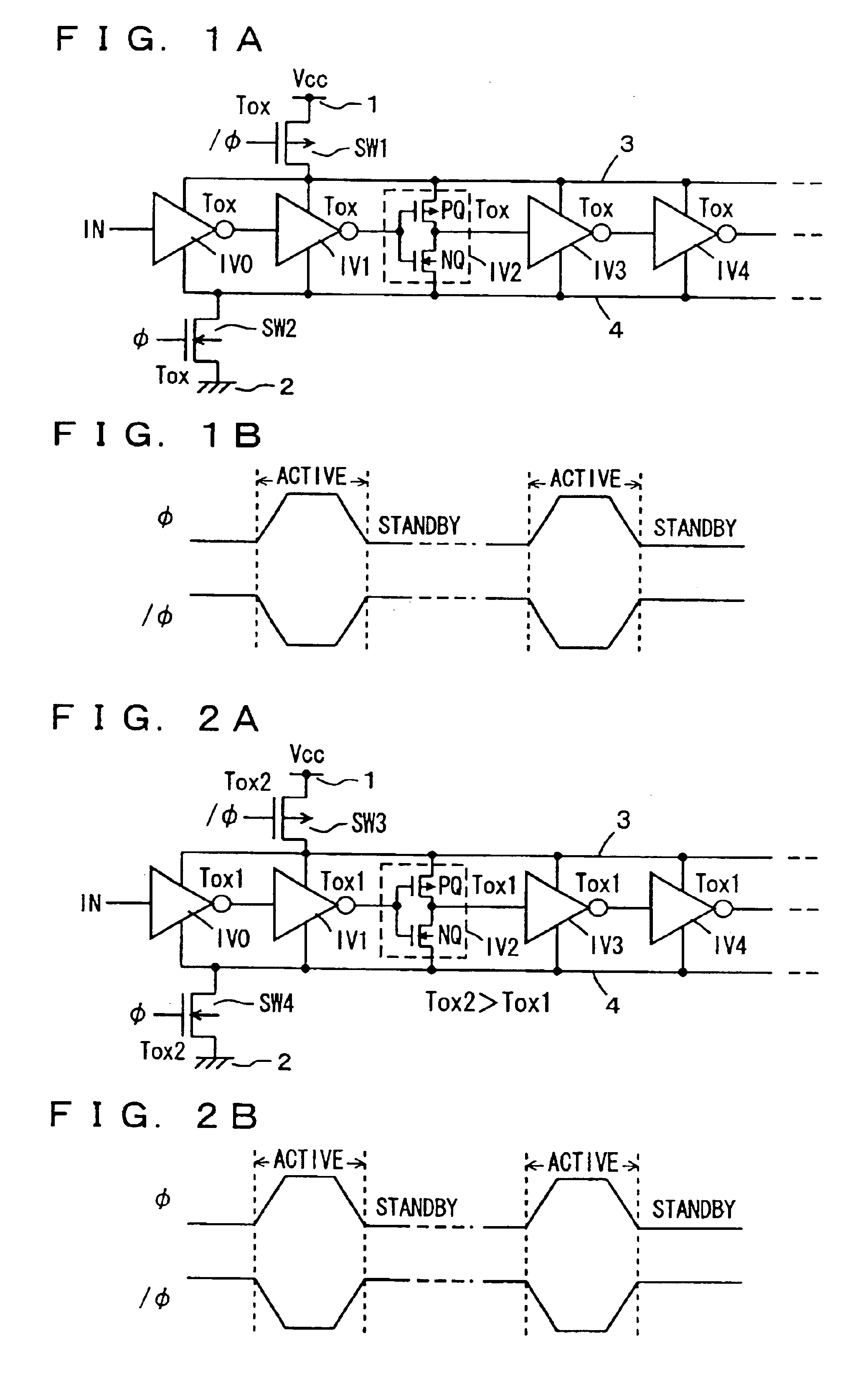
[0157]FIG. 1A schematically shows a structure of a semiconductor device according to a first embodiment of the present invention. Referring to FIG. 1A, the semiconductor device includes cascaded CMOS inverter circuits IV0-IV4. Each of CMOS inverter circuits IV0-IV4 includes a P-channel MIS transistor PQ and an N-channel MIS transistor NQ as its components. Each of MIS transistors PQ and NQ has a gate insulating film having a sufficiently reduced thickness Tox that provides a gate tunnel barrier similar to or lower than a gate tunnel barrier provided, e.g., by a silicon oxide film of 3 nm in thickness. The previous formula of the gate tunnel current J includes the gate insulating film thickness Tox and the barrier height φ as parameters, and therefore, the “gate tunnel barrier” is defined here and hereinafter as being given by a product of thickness Tox of the gate insulating film and a square root of barrier height φ. The barrier height φ is expressed by a di...

second embodiment

[0172][Second Embodiment]

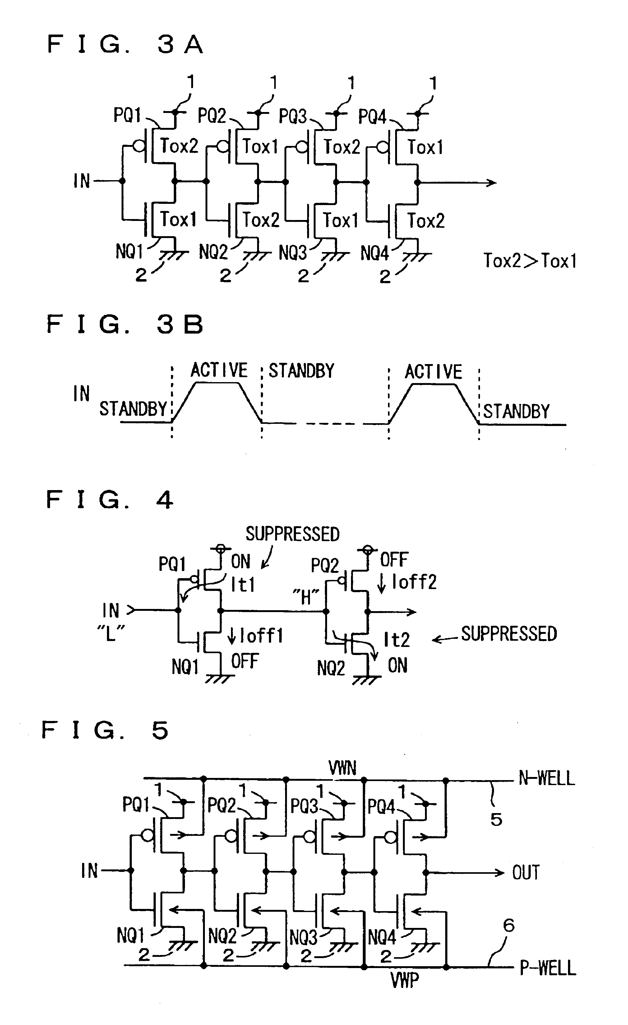
[0173]FIG. 3A schematically shows a structure of a semiconductor device according to a second embodiment of the present invention. In FIG. 3, four CMOS inverter circuits are cascaded. These CMOS inverter circuits are directly coupled to power supply node 1 and ground node 2. More specifically, each of P-channel MIS transistors PQ1-PQ4 has a source coupled to power supply node 1, and each of N-channel MIS transistors NQ1-NQ4 has a source coupled to ground node 2.

[0174]Input signal IN is held at L-level in the standby state and is driven to H-level in the active cycle, as shown in FIG. 3B. In accordance with the logical level of input signal IN in the standby cycle, the thickness of the gate insulating film is set to the large value, the thickness Tox2 in each of MIS transistors PQ1, PQ3, NQ2 and NQ4, which are on in the standby state. In MIS transistors NQ1, PQ2, NQ3 and PQ4 which are off in the standby cycle, the thickness of each gate insulating film is set...

third embodiment

[0178][Third Embodiment]

[0179]FIG. 5 shows a structure of a semiconductor device according to a third embodiment of the present invention. In FIG. 5, four CMOS inverter circuits are arranged. Back gates of P-channel MIS transistors PQ1-PQ4 of these CMOS inverter circuits are commonly connected to an N-well 5, and sources thereof are commonly connected to power supply node 1. Each of N-channel MIS transistors NQ1-NQ4 has a source connected to ground node 2 and a back gate coupled to a P-well 6. A well voltage VWN on N-well 5 and a well voltage VWP on P-well 6 change with the operation cycle.

[0180]FIG. 6 is a signal waveform diagram representing an operation of the semiconductor device shown in FIG. 5. In the standby state, as shown in FIG. 6, the voltage VWN applied to N-well 5 is set to a high voltage Vpp level, and the voltage VWP applied to P-well 6 is set to a negative voltage VBB level. In the active cycle, the voltage VWN applied to N-well 5 is at power supply voltage VCC level...


PUM


Abstract

Transistors having large gate tunnel barriers are used as transistors to be on in a standby state, MIS transistors having thin gate insulating films are used as transistors to be off in the standby state, and main and sub-power supply lines and main and sub-ground lines forming a hierarchical power supply structure are isolated from each other in the standby state so that a gate tunnel current is reduced in the standby state in which a low power consumption is required. In general, a gate tunnel current reducing mechanism is provided for any circuitry operating in a standby state and an active state, and is activated in the standby state to reduce the gate tunnel current in the circuitry in the standby state, to reduce power consumption in the standby state.

Description

[0001]This application is a divisional of application Ser. No. 09 / 776,681 filed Feb. 6, 2001, now U.S. Pat. No. 6,635,934.BACKGROUND OF THE PRESENT INVENTION[0002]1. Field of the Present Invention[0003]The present invention relates to a semiconductor device including insulated gate field effect transistors, referred to as “MIS transistors” hereinafter, as it components, and particularly to a configuration for reducing power consumption in a semiconductor device having miniaturized CMOS transistors (P- and N-channel MIS transistors). More particularly, the present invention relates to a structure for suppressing a gate tunnel current of a miniaturized MIS transistor.[0004]2. Description of the Background Art[0005]In a CMOS semiconductor device, as the size of MIS transistors is reduced, an operation power supply voltage is lowered for ensuring reliability of the transistors and reducing power consumption. For reducing the sizes of MIS transistors in accordance with lowering of the op...

Claims


Application Information

Patent Timeline
IPC IPC(8): H03K19/00H01L21/822G11C11/403G11C11/407H01L21/8238H01L21/8242H01L27/04H01L27/08H01L27/092H01L27/108H01L29/786H03K19/0175H03K19/094
CPCH03K19/0016H01L29/78B82Y10/00
Inventor HIDAKA, HIDETO
Owner RENESAS ELECTRONICS CORP
Why Eureka
Try Eureka