Method and system for floor planning non Manhattan semiconductor integrated circuits

a technology of semiconductor integrated circuits and floor plans, applied in the field of floor plans for non-manhattan semiconductor integrated circuits, can solve problems such as certain not optimal, and achieve the effects of improving the placement, die size, and improving the wiring density of non-manhattan wiring

Inactive Publication Date: 2005-06-28
CADENCE DESIGN SYST INC
View PDF39 Cites 19 Cited by
  • Summary
  • Abstract
  • Description
  • Claims
  • Application Information

AI Technical Summary

Benefits of technology

[0008]The present invention introduces methods of creating floor plans and placements for non Manhattan integrated circuits with existing electronic design automation tools. To create a floor plan, an existing Manhattan based floor planning tool is used. The die size for the floor plan is reduced to take into account the improved wiring density of non Manhattan wiring. A non Manhattan global router is then used on the floor plan to create pin placements. The floor plan may create a floor plan having circuit modules with beveled corners to take advantage of diagonal wiring. To create a placement, an existing Manhattan based placer is first used to create an initial placement. The initial placement is then processed by a non Manhattan aware post processor. The post processor performs local optimizations on the initial placement to improve the placement for a non Manhattan routed integrated circuit.

Problems solved by technology

The Manhattan wiring model has proven to be useful, but it is certainly not optimal.

Method used


Image

  • Method and system for floor planning non Manhattan semiconductor integrated circuits
  • Method and system for floor planning non Manhattan semiconductor integrated circuits
  • Method and system for floor planning non Manhattan semiconductor integrated circuits

Examples


Embodiment Construction

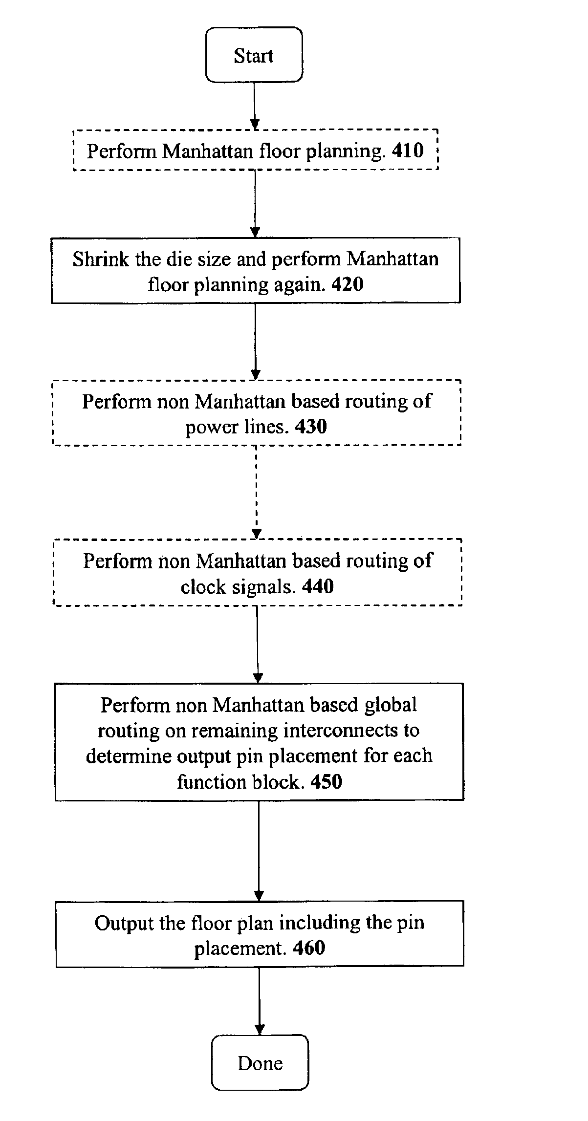
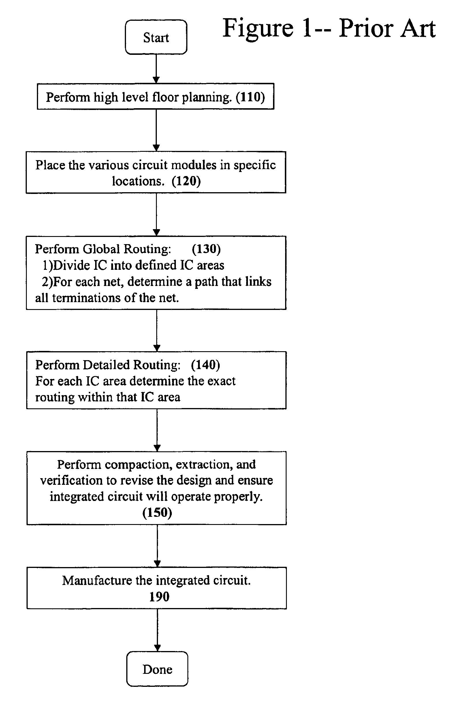
[0031]Methods and systems for floor planning circuit blocks and placing individual circuit cells on non Manhattan semiconductor integrated circuits are disclosed. In the following description, for purposes of explanation, specific nomenclature is set forth to provide a thorough understanding of the present invention. However, it will be apparent to one skilled in the art that these specific details are not required in order to practice the present invention. For example, the present invention discloses a placement post-processor that only considers local optimizations. However, other types of post-processors may be used.

Routing Architectures

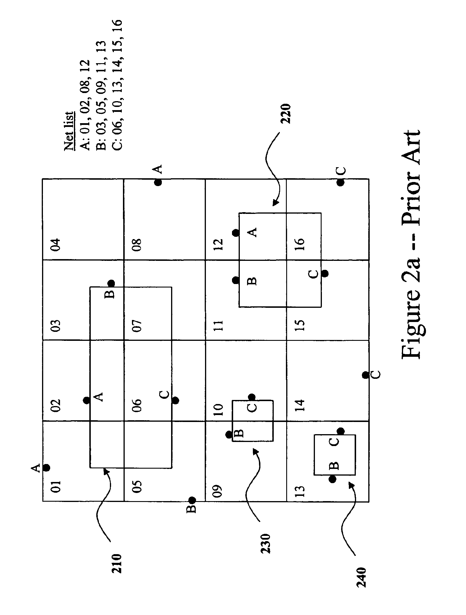
[0032]Most existing semiconductors use the “Manhattan” wiring model that specifies alternating layers of preferred-direction horizontal and vertical wiring. In the Manhattan wiring model, the majority of the interconnect signals are horizontal or vertical. However, occasional diagonal jogs are sometimes allowed on the preferred horizontal and ver...


PUM


Abstract

The present invention introduces methods of creating floor plans and placements for non Manhattan integrated circuits with existing electronic design automation tools. To create a floor plan, an existing Manhattan based floor planning tool is used. The die size for the floor plan is reduced to take into account the improved wiring density of non Manhattan wiring. A non Manhattan global router is then used on the floor plan to create pin placements. The floor plan may create a floor plan having circuit modules with beveled corners to take advantage of diagonal wiring. To create a placement, an existing Manhattan based placer is first used to create an initial placement. The initial placement is then processed by a non Manhattan aware post processor. The post processor performs local optimizations on the initial placement to improve the placement for a non Manhattan routed integrated circuit.

Description

FIELD OF THE INVENTION[0001]The present invention relates to the field of semiconductor design and manufacture. In particular the present invention discloses methods and systems for floor planning circuit blocks and placing individual circuit cells on a non Manhattan semiconductor integrated circuit.BACKGROUND OF THE INVENTION[0002]An integrated circuit (“IC”) is a semiconductor device that includes many electronic components (e.g., transistors, diodes, inverters, etc.). These electrical components are interconnected to form larger scale circuit components (e.g., gates, cells, memory units, arithmetic units, controllers, decoders, etc.) on the IC. The electronic and circuit components of IC's are jointly referred to below as “components.” An integrated circuit also includes multiple layers of metal and / or polysilicon wiring that interconnect its electronic and circuit components.[0003]Design engineers create an integrated circuit by transforming a circuit description of the integrat...

Claims


Application Information

Patent Timeline
Patent Type & Authority Patents(United States)
IPC IPC(8): G06F17/50
CPCG06F17/5072G06F30/392
Inventor TEIG, STEVEN
Owner CADENCE DESIGN SYST INC
Why Eureka
Try Eureka