Silicon single crystal wafer and method for producing silicon single crystal

a single crystal wafer and silicon technology, applied in the direction of polycrystalline material growth, testing/measurement of semiconductor/solid-state devices, under protective fluids, etc., can solve the problems of oxide dielectric breakdown voltage characteristics and device characteristics, degrading electrical characteristics, and oxide-film defects remarkably, etc., to achieve excellent electrical properties, stable supply, and high breakdown voltage

Inactive Publication Date: 2005-07-05
SHIN-ETSU HANDOTAI CO LTD
View PDF6 Cites 24 Cited by
  • Summary
  • Abstract
  • Description
  • Claims
  • Application Information

AI Technical Summary

Benefits of technology

[0026]As described above, if a pulling rate at the time of a crystal growth is 0.5 mm/min or more, the manufacturing margin wherein the defect-free region of the present invention, especially the region in which an oxide-precipitates layer is formed is enlarged, and thereby a stable supply can be achieved.
[0027]As explained ab...

Problems solved by technology

There exist defects introduced during growth of a single crystal called grown-in defects such as FPD, LSTD and COP, which degrade oxide dielectric breakdown voltage characteristics and device characteristics.
However, it has been found that an oxide-film defects may occur remarkably, even if it is a crystal such a...

Method used


Image

  • Silicon single crystal wafer and method for producing silicon single crystal
  • Silicon single crystal wafer and method for producing silicon single crystal
  • Silicon single crystal wafer and method for producing silicon single crystal

Examples


experiment 1

(Experiment 1)

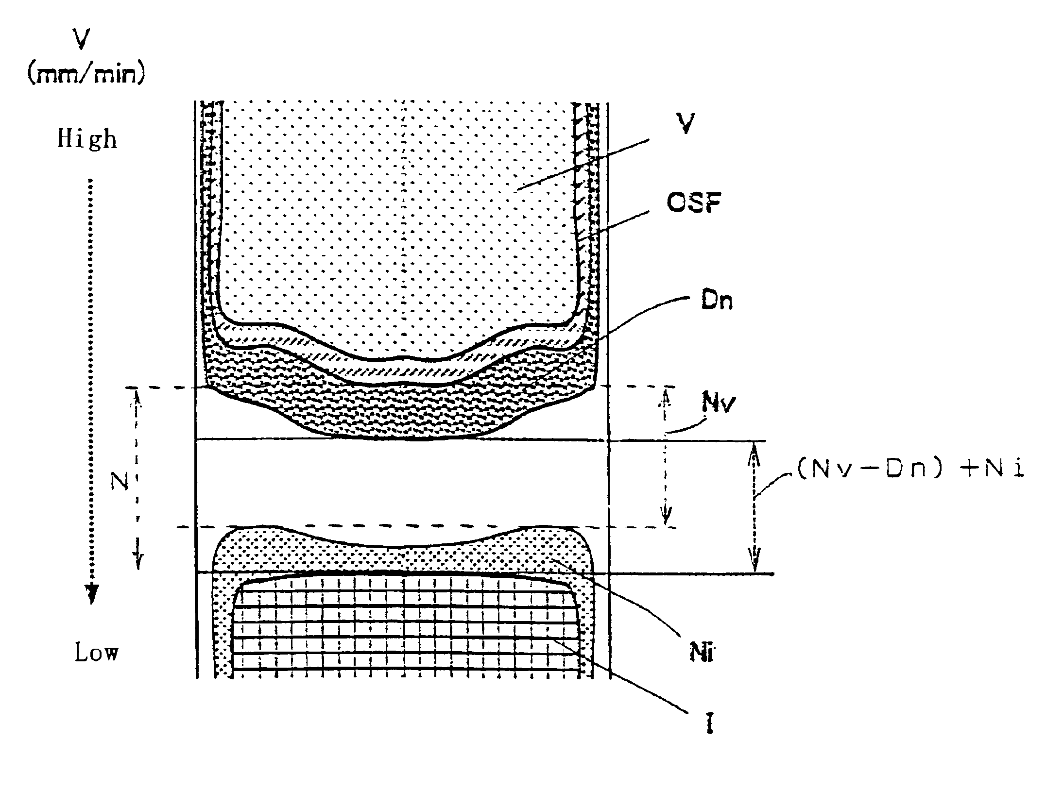
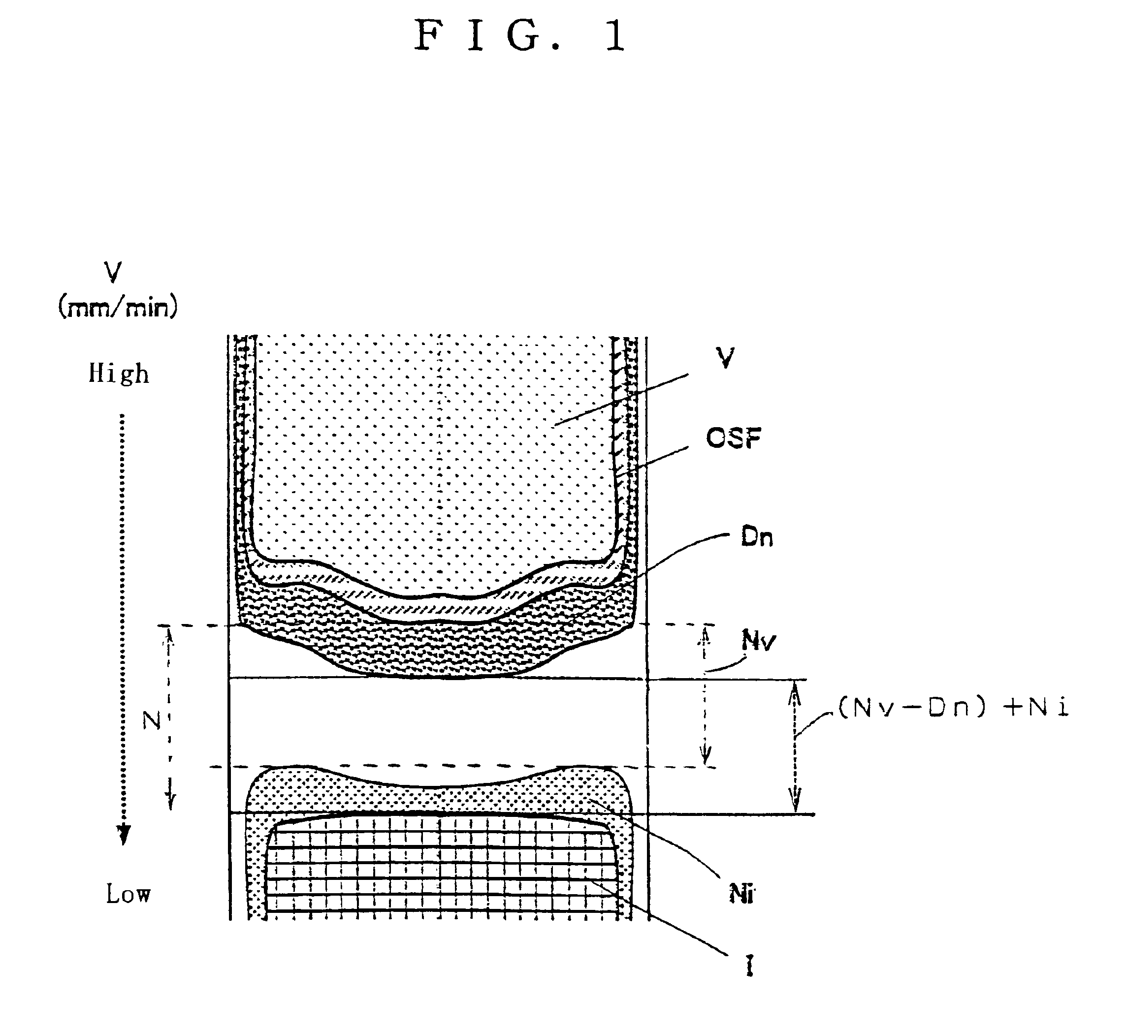
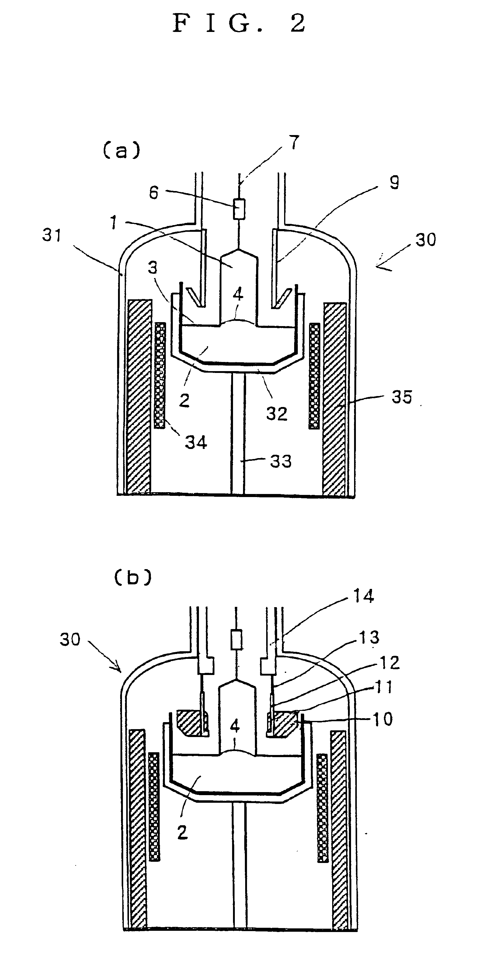
[0058]The MCZ single crystal pulling apparatuses (a horizontal magnetic field is applied) shown as Apparatus A of FIG. 2(a) and Apparatus B of FIG. 2(b) were used. In Apparatus A 150 kg of polycrystal silicon as raw material was charged into a 24 inch quartz crucible. In Apparatus B, 160 kg of polycrystal silicon as raw material was charged into a 26 inch quartz crucible. Then, a silicon single crystal with a diameter of 8 inches (diameter of 200 mm) and orientation was pulled using each of the apparatuses. When pulling the single crystal, a growth rate was gradually lowered from a top to a tail of the crystal in the range of 0.7 mm / min to 0.3 mm / min. The crystal was produced so that the oxygen concentration in the wafer might be 22-23 ppma (ASTM'79 value).

[0059]As shown in FIGS. 3(a) and (b), the pulled crystal was cut parallel to the direction of the crystal growth axis from the head to the tail, to produce four wafer samples. Among four samples, three samples were ...

experiment 2

(Experiment 2)

[0075]Based on the above-mentioned results, using Apparatus B (FIG. 2(b)), a crystal was pulled with controlling a growth rate so that there might be obtained the region which is in N region outside of OSF, is not Cu deposition defect region (Dn region), and does not contain the Ni region where oxygen precipitation is hardly caused. The pulled crystal was processed to be a mirror finished wafer, and oxide dielectric breakdown voltage characteristics were evaluated.

[0076]The C-mode measurement conditions are as follows.[0077]1) Oxide film : 25 nm,[0078]2) measuring electrode: phosphorus doped polysilicon,[0079]3) electrode area: 8 mm2 and[0080]4) current density in decision: 1 mA / cm2.

[0081]As a result, oxide dielectric breakdown voltage level as 100% of good chip yield can be achieved.

[0082]The inventors of the present invention have studied further based on the knowledge acquired in the above experiments, and completed the present invention.

[0083]The first method for p...


PUM


Abstract

There can be provided a silicon single crystal wafer grown according to Czochralski method wherein the whole plane of the wafer is occupied by N region on the outside of OSF generated in a shape of a ring by thermal oxidation treatment and there exists no defect region detected by Cu deposition. Thereby, there can be produced a silicon single crystal wafer according to CZ method, which does not belong to any of V region rich in vacancies, OSF region and I region rich in interstitial silicons, and can surely improve electric characteristics such as oxide dielectric breakdown voltage characteristics or the like under stable manufacture conditions.

Description

TECHNICAL FIELD[0001]The present invention relates to a silicon single crystal wafer with high breakdown voltage and excellent electrical characteristics, in which any of defect regions such as V region, OSF region and I region as described below are not present, and in which oxide-film defects detected by copper deposition treatment are not formed, and a method for producing the silicon single crystal.BACKGROUND TECHNOLOGY[0002]In recent years, a demand for quality of a silicon single crystal produced by Czochralski method (hereafter abbreviated to CZ method) used as a substrate has been increasing due to decrease in size of a device resulting from increased degree of integration of a semiconductor circuit. There exist defects introduced during growth of a single crystal called grown-in defects such as FPD, LSTD and COP, which degrade oxide dielectric breakdown voltage characteristics and device characteristics. It has been considered that it is important to decrease a density and ...

Claims


Application Information

Patent Timeline
IPC IPC(8): C30B15/14C30B15/00C30B29/06H01L21/208H01L21/66
CPCC30B15/14C30B29/06
Inventor SAKURADA, MASAHIROKOBAYASHI, TAKESHIMORI, TATSUOFUSEGAWA, IZUMIOHTA, TOMOHIKO
Owner SHIN-ETSU HANDOTAI CO LTD
Why Eureka
Try Eureka