Multi-chip module, semiconductor chip, and interchip connection test method for multi-chip module

Inactive Publication Date: 2005-07-05
PANASONIC CORP
View PDF5 Cites 91 Cited by
  • Summary
  • Abstract
  • Description
  • Claims
  • Application Information

AI Technical Summary

Benefits of technology

[0035]In addition, in the present invention, a node of the connecting member on the line located between analog and digital signal lines, for example, is grounded by turning the third switch circuit on, and thus the node becomes a low-impedance node. Accordingly, the problem of crosstalk can be avoided. Besi

Problems solved by technology

However, in implementing such a device, the system LSI is confronted with two problems as described below.
A first problem is that the increase in the size of the system LSI requires considerable development efforts and the fabricating cost of the device is increased because its fabricating yield is reduced due to an increase in chip area.
A second problem is that it is hard to carry out the process of combining different types of devices (including a DRAM and a flash memory, for example) on a chip in coordination with the process of fabricating a pure CMOS, thus making it very difficult to put both the processes into practice at the same time.
Therefore, the process of combining different types of devices on a chip falls behind the most advanced pure CMOS fabricating process in development for about one or two years, which prevents production and supply

Method used


Image

  • Multi-chip module, semiconductor chip, and interchip connection test method for multi-chip module
  • Multi-chip module, semiconductor chip, and interchip connection test method for multi-chip module
  • Multi-chip module, semiconductor chip, and interchip connection test method for multi-chip module

Examples


first embodiment

[0063](First Embodiment)

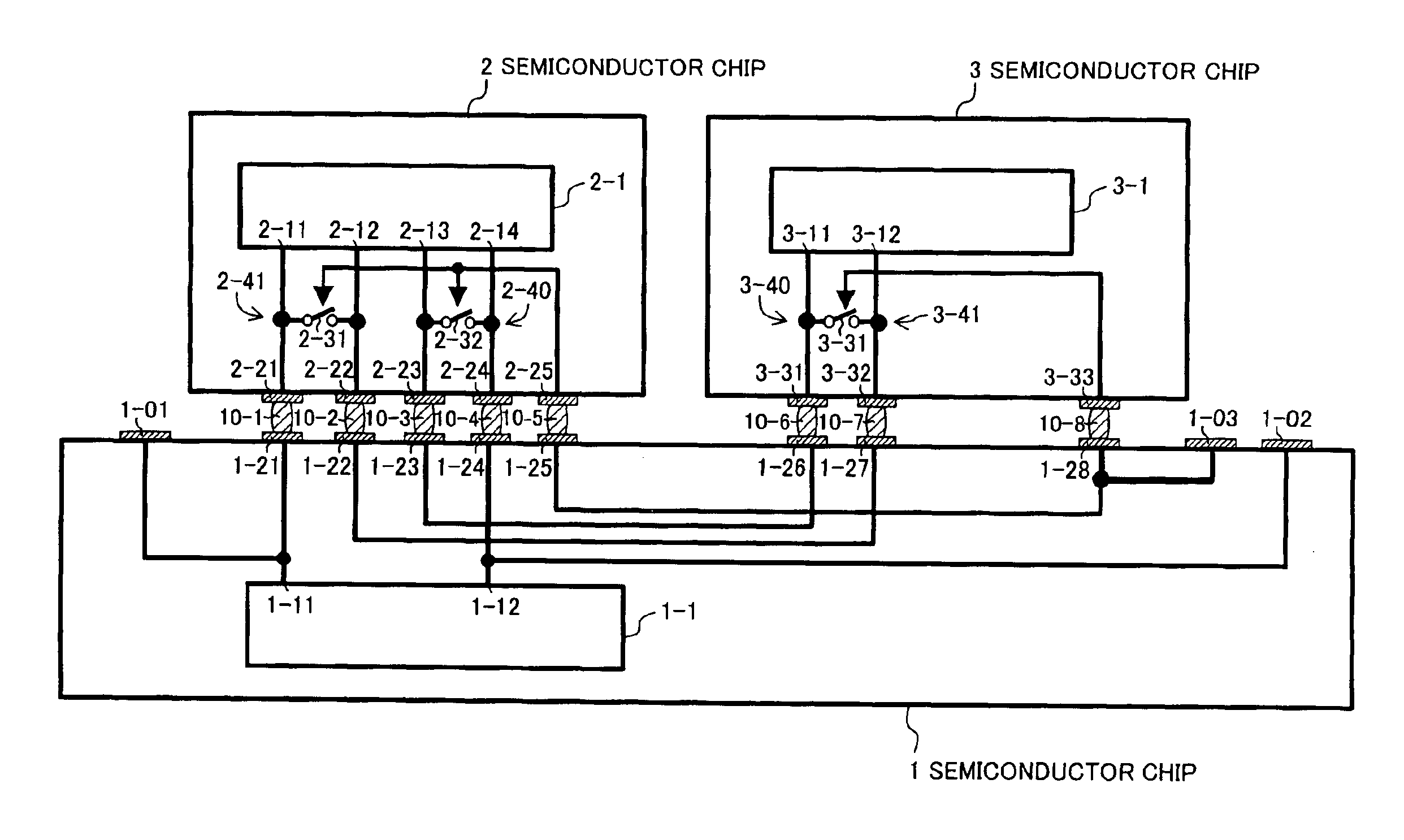
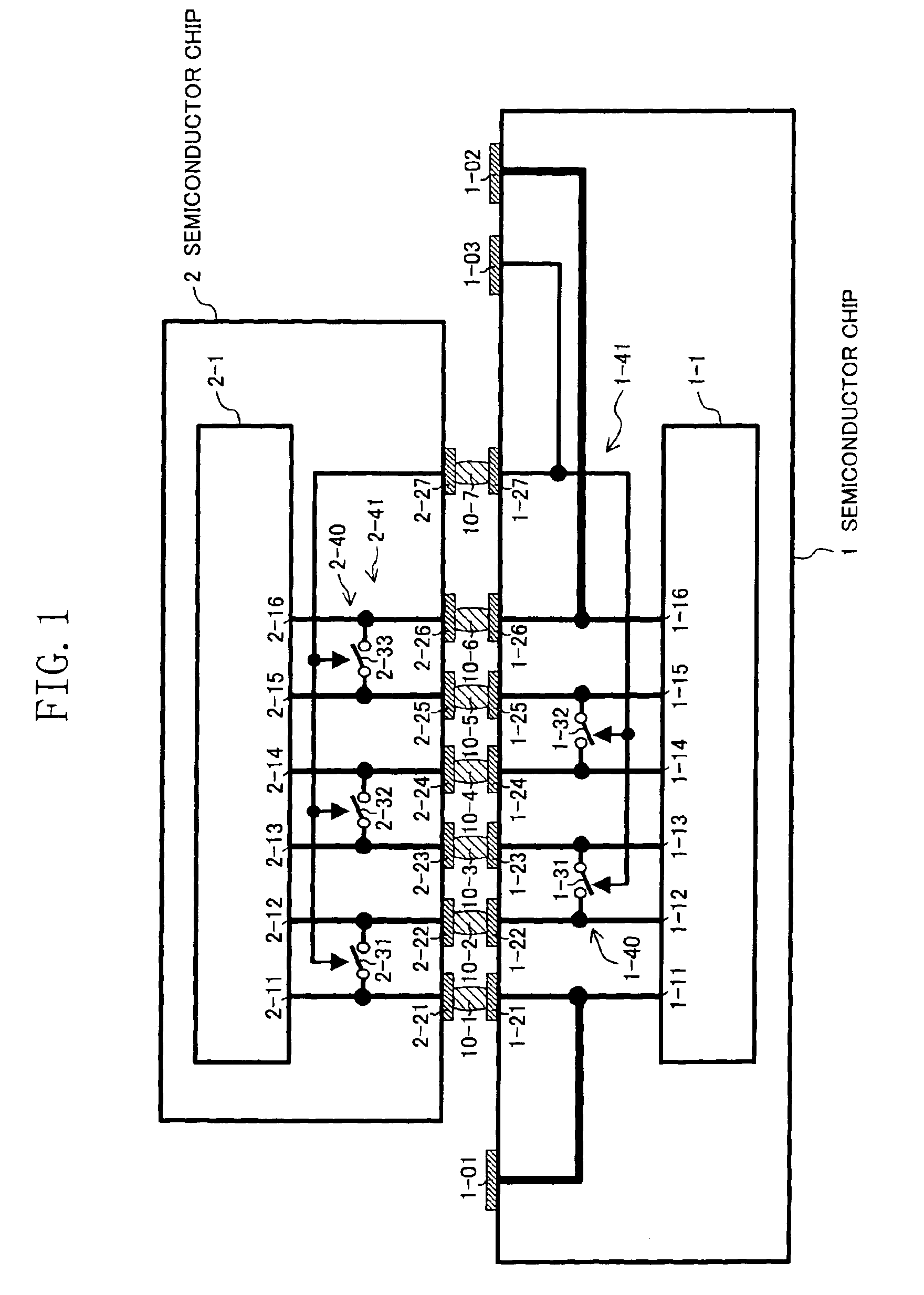
[0064]FIG. 1 shows the overall configuration of a chip-on-chip (hereinafter, abbreviated as COC) type multi-chip module according to a first embodiment of the present invention. That is, FIG. 1 shows an exemplary circuit configuration of a multi-chip module to which the present invention is applied, wherein the multi-chip module includes a semiconductor chip 1 having an internal circuit 1-1 and a semiconductor chip 2 having an internal circuit 2-1, the internal circuits 1-1 and 2-1 are provided with signal terminals 1-11 through 1-16 and signal terminals 2-11 through 2-16, respectively, and the signal terminals 1-11 through 1-16 are connected to the signal terminals 2-11 through 2-16, respectively, thus implementing the multi-chip module.

[0065]In FIG. 1, the signal terminal 1-11 is electrically connected to the connection pad 1-21 provided on the semiconductor chip 1, and the signal terminal 2-11 is electrically connected to the connection pad 2-21 provided o...

second embodiment

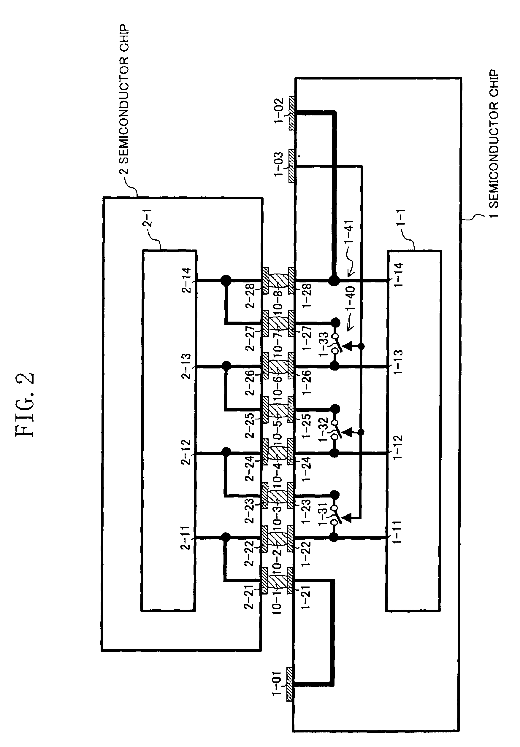
[0072](Second Embodiment)

[0073]FIG. 2 shows a multi-chip module according to a second embodiment of the present invention. Although the test control circuits 1-41 and 2-41 can be provided in the master and slave semiconductor chips 1 and 2, respectively, in the first embodiment, the test control circuit is provided only in a semiconductor chip 1 in the present embodiment. It should be noted that in FIG. 2, the same components are identified by the same reference characters as those used in FIG. 1.

[0074]FIG. 2 shows an exemplary circuit configuration of a multi-chip module which is implemented by connecting signal terminals 1-11 through 1-14 of an internal circuit 1-1 in the semiconductor chip 1 to signal terminals 2-11 through 2-14 of an internal circuit 2-1 in a semiconductor chip 2.

[0075]The feature of the present embodiment is that the slave chip (first semiconductor chip) 2 is provided with no test control circuit 2-41 unlike the first embodiment, but the signal terminals 2-11 t...

third embodiment

[0081](Third Embodiment)

[0082]FIG. 3 shows a multi-chip module according to a third embodiment of the present invention. In the second embodiment, only the semiconductor chip 1 is provided with the test control circuit, that is, the switch elements are inserted into only the semiconductor chip 1. To the contrary, in the third embodiment, only the semiconductor chip 2 is provided with switch elements. Other than this point, the operating principle and effects of the multi-chip module are exactly the same as those of the second embodiment. Accordingly, those skilled in the art can easily understand the operating principle, and therefore the detailed description thereof will be omitted.


PUM


Abstract

A multi-chip module is implemented by connecting a plurality of connection pads provided on, for example, two semiconductor chips via a plurality of conductive connecting members. To carry out a test for determining the quality of the connection between the two semiconductor chips, the multi-chip module is further provided with a plurality of switch elements so that the plurality of connecting members can be electrically conducted in a serial manner via the connection pads of the semiconductor chips. During the connection test, all the switch elements are turned on, and the impedance between both ends of the line including the plurality of connecting members conducted in a serial manner is measured using two probing pads.

Description

BACKGROUND OF THE INVENTION[0001]The present invention relates to multi-chip modules that include a plurality of semiconductor chips having a plurality of connection pads and that are implemented by electrically connecting the associated connection pads to each other between the semiconductor chips. The present invention also relates to semiconductor chips for use in forming such multi-chip modules, and test methods for the connection between the semiconductor chips in the multi-chip modules.[0002]In recent years, the concept of a so-called one-chip system LSI in which a plurality of functional elements are formed on a common substrate has been introduced, and various propositions have been made for methods of designing such system LSIs. In particular, the advantage of the one-chip system LSI is that a variety of functional elements such as a memory (e.g., DRAM or SRAM), a logic circuit, and an analogue circuit can be integrated on a single semiconductor chip, thus implementing a hi...

Claims


Application Information

Patent Timeline
IPC IPC(8): G01R31/28G01R31/3185H01L25/18H01L21/822H01L23/52H01L27/04
CPCG01R31/2853G01R31/318505G01R31/318513G11C29/022H01L25/18H01L2924/3011H01L2224/16145H01L2224/05573H01L2224/05568H01L2924/00014H01L2224/05599
Inventor SAKIYAMA, SHIROKINOSHITA, MASAYOSHIKAJIWARA, JUN
Owner PANASONIC CORP
Why Eureka
Try Eureka