Semiconductor device, a method of manufacturing the semiconductor device and a method of deleting information from the semiconductor device

Inactive Publication Date: 2005-07-12
UNITED MICROELECTRONICS CORP
View PDF19 Cites 19 Cited by
  • Summary
  • Abstract
  • Description
  • Claims
  • Application Information

AI Technical Summary

Benefits of technology

[0027]It is an object of the present invention to provide a semiconductor device which increases the process margin without being affected by close location of element isolat

Problems solved by technology

However, the following problems are posed in gate electrode formation.
In addition, this technique requires an extra polishing process to the manufacturing processes and therefore cannot meet one of important requirements associated with manufacturing of the semiconductor device, i.e., reduction of the number of processes.
However, when the width of the gate electrode wiring layer is reduced to the exposure limit, the resist pattern used to separate the pad polysilicon films on the gate electrode has a width equal to or smaller than the exposure limit, so the pad polysilicon films are hard to be patterned by photolithography processes.
For this reason, conventionally, the width of the gate electrode wiring pattern cannot be reduced to the exposure limit, thus impeding micropatterning of a semiconductor device.
However, the cumbersome processes as described above are required to form th

Method used


Image

  • Semiconductor device, a method of manufacturing the semiconductor device and a method of deleting information from the semiconductor device
  • Semiconductor device, a method of manufacturing the semiconductor device and a method of deleting information from the semiconductor device
  • Semiconductor device, a method of manufacturing the semiconductor device and a method of deleting information from the semiconductor device

Examples


first embodiment -

[0114]-First Embodiment-

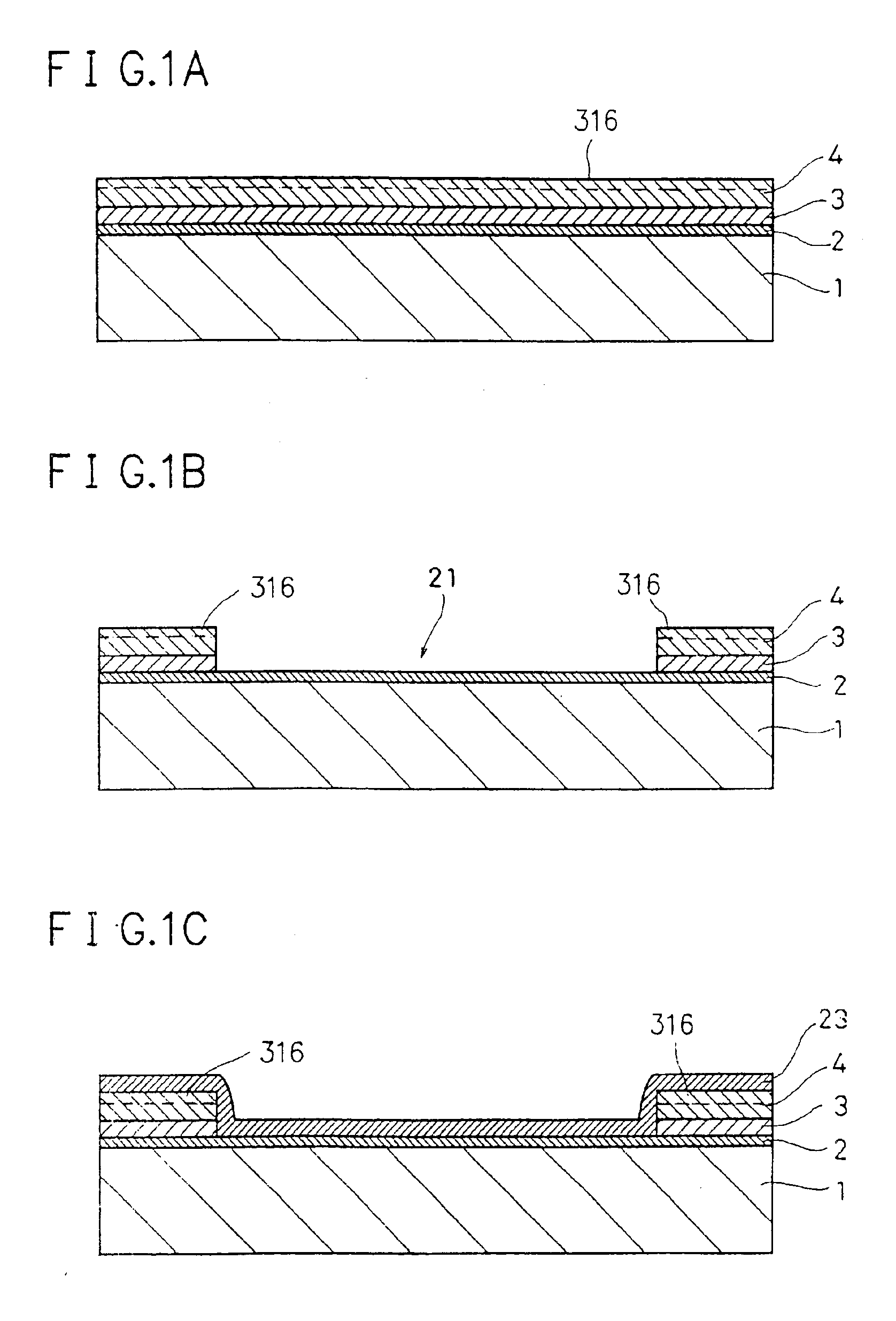
[0115]The first embodiment will be described first. In the first embodiment, an example in which the present invention is applied to a MOS transistor will be described. In the first embodiment, the structure of the MOS transistor and a manufacturing method therefor will be described together. FIGS. 1A to 1J are schematic sectional views showing steps in manufacturing the MOS transistor.

[0116]An element isolation structure is formed in an element isolation region on a p-type silicon semiconductor substrate by a so-called field shield element isolation method, thereby demarcating an element formation region.

[0117]More specifically, as shown in FIG. 1A, a silicon oxide film 2, a polysilicon film 3, and a silicon oxide film 4 are formed on a p-type silicon semiconductor substrate 1 to thicknesses of, e.g., about 50 nm, 200 nm, and 200 nm, respectively. A silicon nitride film 316 having a thickness of about 200 nm may be formed on the entire surface of the silicon...

second embodiment -

[0130]-Second Embodiment-

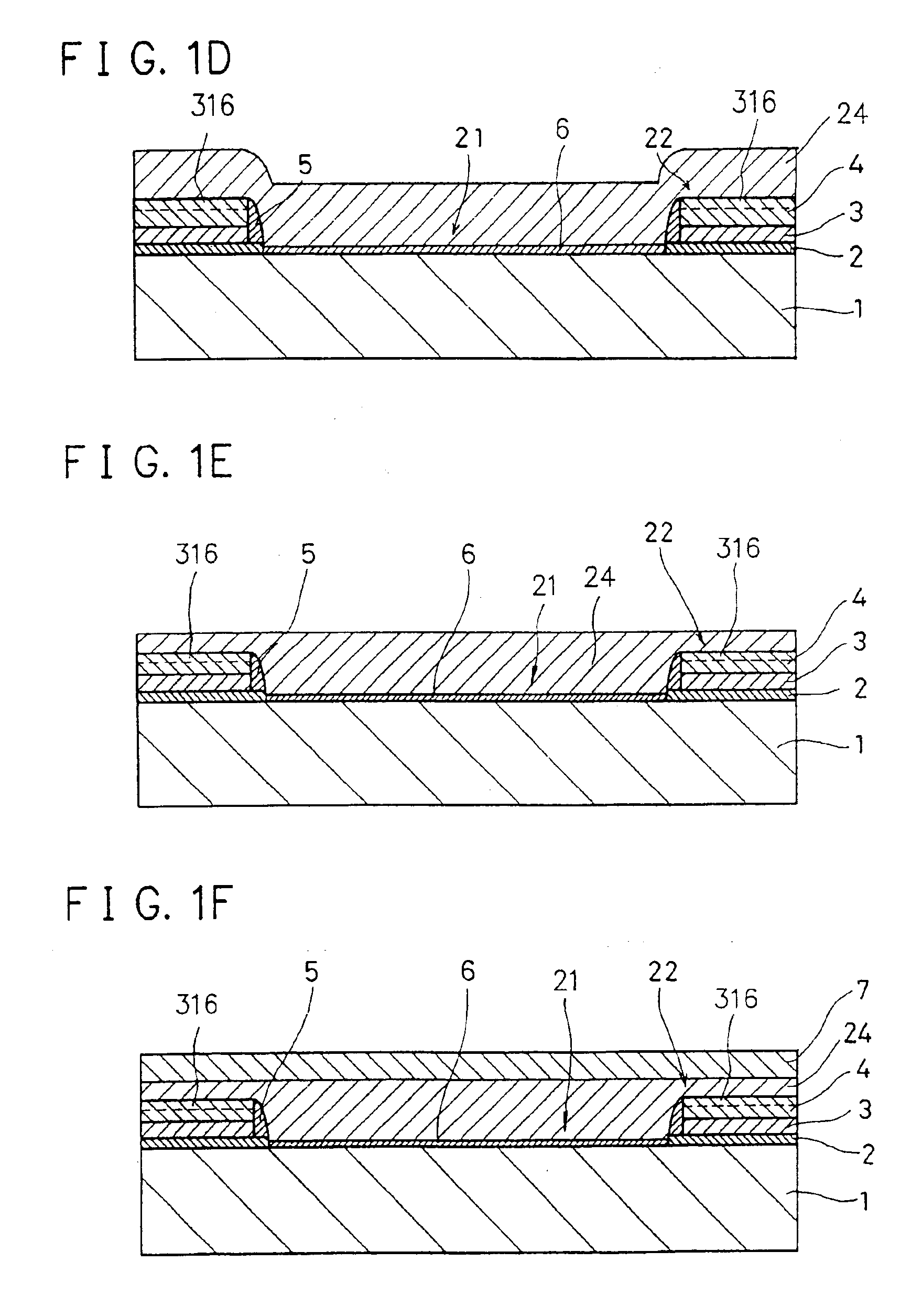
[0131]The second embodiment will be described next. As in the first embodiment, the structure of a MOS transistor and a manufacturing method therefor will be described together. The second embodiment is slightly different in the surface polishing method. A detailed description of the same steps as in the first embodiment will be omitted. The same reference numerals as in the first embodiment denote the same constituent elements in the second embodiment, and a detailed description thereof will be omitted.

[0132]In the second embodiment, in steps shown in FIGS. 1E and 1F of the above-described first embodiment, to easily and properly control polishing of a polysilicon film 24, silicon oxide films 4 serving as cap insulating films of field shield element isolation structures 22 are used as stoppers. When the cap insulating film is formed as an multilayered insulating film consisting of the silicon oxide film 4 and a silicon nitride film 316, the silicon nitride ...

third embodiment -

[0144]-Third Embodiment-

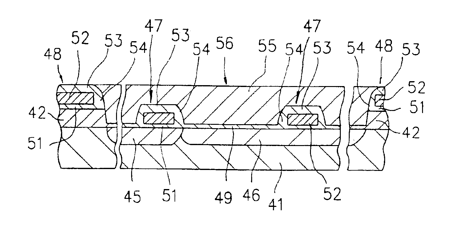
[0145]The third embodiment of the present invention will be described below. In the third embodiment, an example in which a semiconductor device according to the present invention and a manufacturing method therefor are applied to a MOS transistor will be described, as in the first embodiment. In the third embodiment, the structure of the MOS transistor and steps in manufacturing the MOS transistor will be described together. FIGS. 4A to 4G are schematic sectional views showing steps in manufacturing the MOS transistor of the third embodiment.

[0146]First, p- and n-type wells are formed in the surface region of a p-type silicon semiconductor substrate.

[0147]More specifically, as shown in FIG. 4A, the entire surface of a p-type silicon semiconductor substrate 41 is subjected to thermal oxidation to form a silicon oxide film (so-called preoxide film) 42 having a thickness of about 1,000 to 5,000 Å. A resist 43 is applied to the surface of the silicon oxide film ...


PUM


Abstract

A semiconductor device and a method for manufacturing the same and method for deleting information in use of the semiconductor device, in which field shield isolation or a trench type isolation between elements is used with suppression of penetration of field oxide into element active region of the device, that is, a defect involved in conventional LOCOS type process, are disclosed. A non-LOCOS insulating device isolation block is formed in a semiconductor substrate. The non-LOCOS insulating device isolation block uses a field shield element isolation structure or trench type element isolation structure. After gate electrode wiring layers are formed in a field region and an active region to the same level, a pad polysilicon film formed on the entire surface to cover the patterns of these gate electrode wiring layers is polished by chemical mechanical polishing (CMP) using the cap insulating films of the gate electrode wiring layers as stoppers, thereby forming the gate electrode wiring layers into separated patterns. With this arrangement, even when the width of the gate electrode wiring layer is reduced to the exposure limit in photolithography, the pad polysilicon film can be separated and patterned.

Description

CROSS-REFERENCE TO RELATED APPLICATIONS[0001]This application is a Division of U.S. patent application Ser. No. 09 / 379,802 filed on Aug. 24, 1999 now U.S. Pat. No. 6,657,229 by Eguchi, et al. entitled SEMICONDUCTOR DEVICE, A METHOD OF MANUFACTURING THE SEMICONDUCTOR DEVICE AND A METHOD OF DELETING INFORMATION FROM THE SEMICONDUCTOR DEVICE which was a Division of U.S. patent application Ser. No. 08 / 864,796 filed on May 28, 1997 by Eguchi, et al entitled SEMICONDUCTOR DEVICE, A METHOD OF MANUFACTURING THE SEMICONDUCTOR DEVICE AND A METHOD OF DELETING INFORMATION FROM THE SEMICONDUCTOR DEVICE, now abandoned, the entire contents of each of which are incorporated by reference, and for which priority is claimed under 35 U.S.C. §120. As in parent U.S. patent application Ser. No. 08 / 864,796, priority is also claimed under 35 U.S.C. §119 to JP 8-156266 filed on May 28, 1996; JP8-195437 filed on Jul. 5, 1996; JP8-293369 filed on Oct. 15, 1996; 9-19860 filed on Jan. 17, 1997; and JP9-119884 fi...

Claims


Application Information

Patent Timeline
IPC IPC(8): H01L21/765H01L27/115H01L21/70H01L21/761H01L21/822H01L21/8247H01L27/06H01L27/148
CPCH01L21/761H01L21/765H01L21/8221H01L27/0688H01L27/115H01L27/11521H01L27/11551H01L27/1463H10B41/20H10B69/00H10B41/30
Inventor EGUCHI, KOHEIEGAWA, YUICHIIWASA, SHOICHIFUJIKAKE, HIDEKIYOKOZEKI, WATARUKAWAMATA, TATSUYA
Owner UNITED MICROELECTRONICS CORP
Why Eureka
Try Eureka