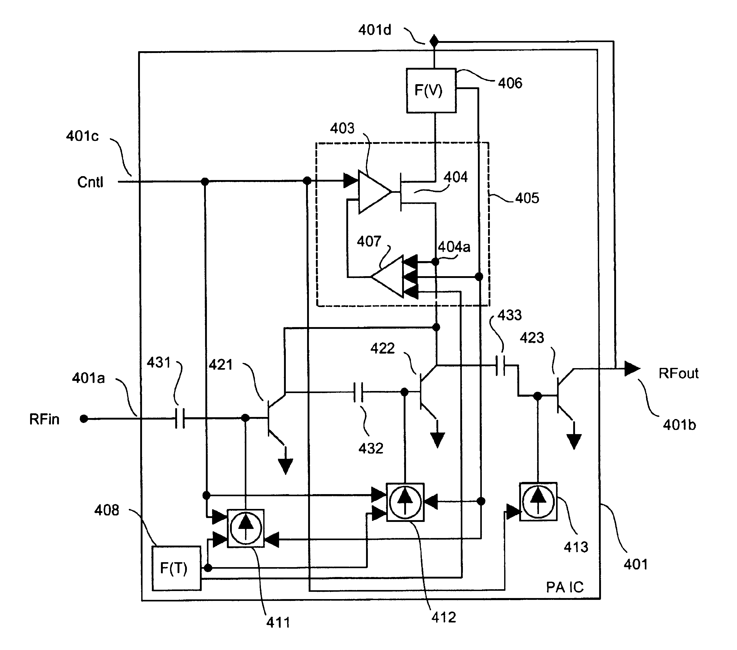
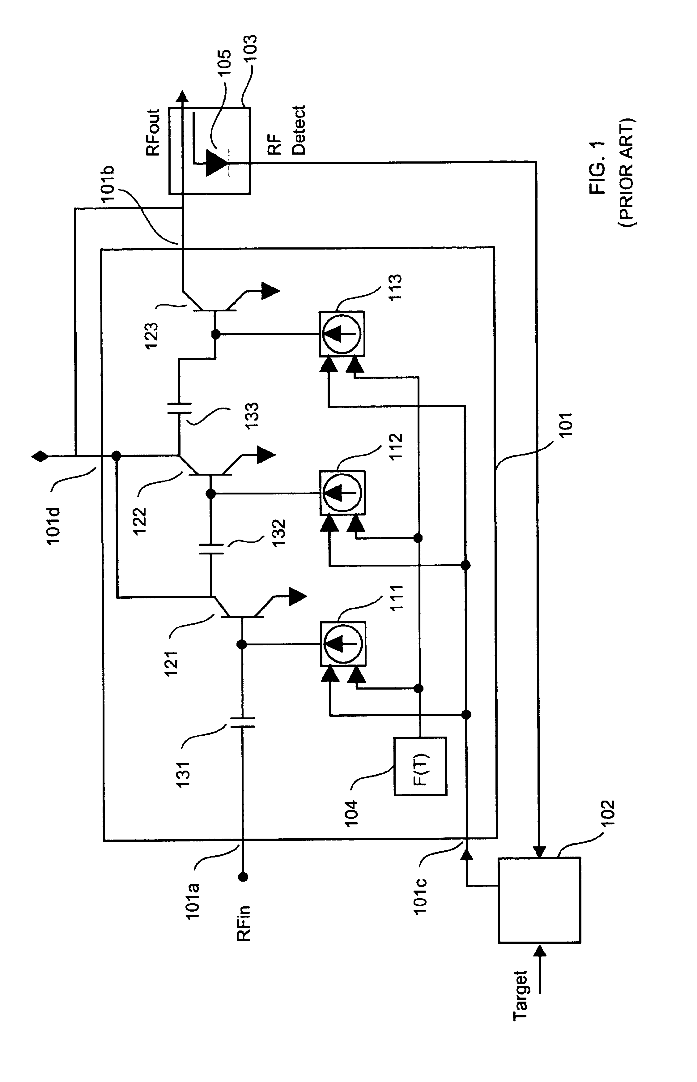
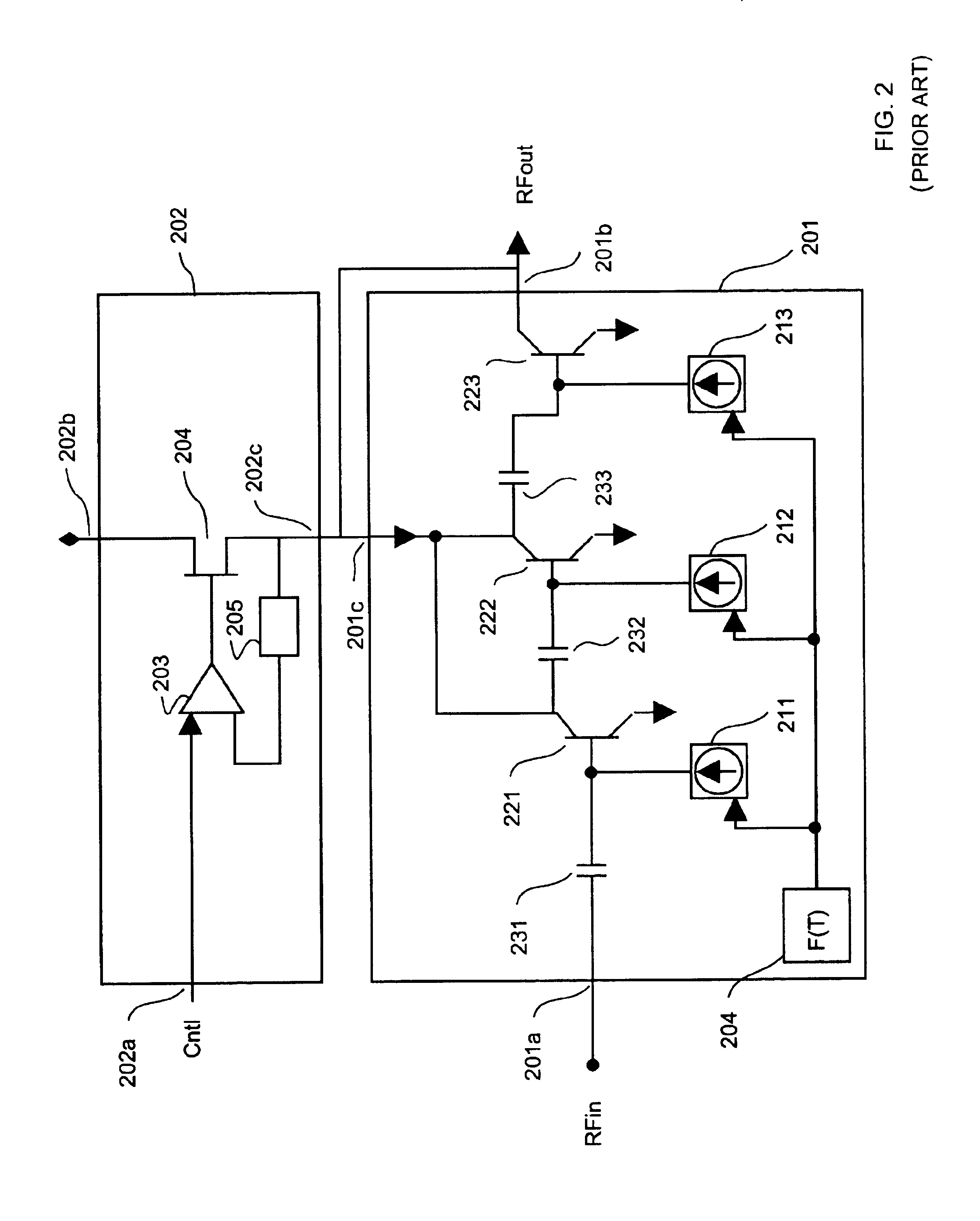
[0011]In accordance with the invention there is provided a power amplifier circuit comprising: an input port for receiving a RF input signal; an output port for providing a RF output signal therefrom that is an amplified version of the RF input signal; a control port for receiving a control signal; a supply voltage input port for receiving a supply voltage; a temperature sensing circuit for sensing a temperature of the power amplifier circuit and for providing a temperature signal in dependence thereon; a voltage sensing circuit for sensing a potential of a voltage supply and for providing a sense signal in dependence thereon; a first amplification stage having a first gain for amplifying one of a signal derived from the RF input signal and the RF input signal to form a first amplified RF signal, the first amplification stage for receiving at least one of the temperature signal and the sense signal and the control signal and for varying the first gain in dependence thereon; and, a second amplification stage having a second gain for amplifying one of a signal derived from the first amplified RF signal and the first amplified RF signal to form the RF output signal, the second amplification stage for receiving the control signal and other than receiving at least one of the temperature signal and the sense signal for varying the second gain in dependence thereon.
[0012]In accordance with the invention there is provided a method of operating a multi amplification stage amplifier circuit comprising the steps of: receiving of a control signal having a control signal magnitude; providing a first amplification stage having a first gain; receiving one of a signal derived from a RF input signal and a RF input signal for amplification using the first amplification stage; amplifying the one of a signal derived from the RF input signal and the RF input signal using the first amplification stage to form a first amplified RF signal, the amplifying of the one of a signal derived from the RF input signal and the RF input signal performed in conjunction with a step of compensating of the first amplification stage for at least two of temperature and supply voltage and control signal magnitude; providing a second amplification stage having a second gain; receiving of the first amplified RF signal using the second amplification stage; and, amplifying one of a signal derived from the first amplified RF signal and the first amplified signal using the second amplification stage to form a RF output signal, the amplifying of the one of a signal derived from the first amplified RF signal and the first amplified signal performed in conjunction with a step of other than compensating of the second amplification stage for at least one of temperature and supply voltage fluctuations.
[0013]In accordance with the invention there is provided a power amplifier circuit comprising: an input port for receiving a RF input signal; an output port for providing a RF output signal therefrom that is an amplified version of the RF input signal; a control port for receiving a control signal; a supply voltage input port for receiving a supply voltage; a temperature sensing circuit for sensing a temperature of the power amplifier circuit and for providing a temperature signal in dependence thereon; a voltage sensing circuit for sensing a potential of a voltage supply and for providing a sense signal in dependence thereon; a first amplification stage having a first gain and for amplifying one of a signal derived from the RF input signal and the RF input signal to form a first amplified signal, the first amplification stage for receiving at least one of the temperature signal and the sense signal and the control signal and for varying the first gain in dependence thereon; and, a second amplification stage having a second gain and for amplifying one of a signal derived from the first amplified signal the first amplified signal, the second amplification stage for receiving at least one of the control signal and the temperature signal and the sense signal for varying the second gain in dependence thereon, the second amplification stage coupled directly to the supply voltage input port.
[0014]In accordance with the invention there is provided a method of operating a poly stage amplifier circuit comprising the steps of: providing of a first amplification stage having a first gain and for receiving one of a signal derived from a RF input signal and a RF input signal for amplification; amplifying the one of a signal derived from the RF input signal and the RF input signal using the first amplification stage to form a first amplified signal, the amplifying of the one of a signal derived from the RF input signal and the RF input signal performed in conjunction with a step of compensating of the first amplification stage for at least one of temperature and supply voltage fluctuation and control signal magnitude; providing of a second amplification stage having a second gain and for receiving one of a signal derived from the first amplified signal and the first amplified signal; supplying the supply voltage to the second amplification stage without a substantial voltage drop between a potential of the supply voltage and that received by the second amplifying stage; and, amplifying the signal derived from the first amplified signal and the first amplified signal using the second amplification stage to form a RF output signal, the amplifying of the signal derived from the first amplified signal and the first amplified signal performed in conjunction with a step of compensating of the second amplification stage for at least one of temperature and supply voltage fluctuations.
[0015]In accordance with the invention there is provided an amplifier circuit for receiving an input signal for amplification comprising: an input port for receiving a RF input signal; an output port for providing a RF output signal therefrom that is an amplified version of the RF input signal; a control port for receiving a control signal; a supply voltage input port for receiving a supply voltage; a regulator circuit for receiving the supply voltage and for providing a regulated supply voltage in dependence upon at least one of a temperature of the amplifier circuit, the supply voltage, and the regulated supply voltage, where at least one of the temperature signal, the supply voltage and the regulated supply voltage are provided to the regulator circuit using a direct feedback path; at least a first amplification stage and a second amplification stage, the at least a first amplification stage and the second amplification stage coupled to at least one of the supply voltage and the regulated supply voltage, the first amplification stage for receiving one of a signal derived from the RF input signal and the RF input signal and for providing a first amplified signal, to the second amplification stage, the second amplification stage for amplifying a signal derived from the first amplified signal and the first amplified signal to form the RF output signal.
[0016]In accordance with the invention there is provided a method of operating a multi stage amplifier circuit comprising the steps of: receiving a RF input signal; receiving a supply voltage; receiving a control signal; receiving at least one of a temperature signal related to a temperature of the amplifier circuit and a sense signal related to the supply voltage; regulating the received supply voltage to form a regulated supply voltage in dependence upon the received at least one of temperature signal and sense signal; providing a first amplification stage having a first gain; providing a second amplification stage having a second gain; providing the regulated supply voltage to at lease one of the first amplification stage and the second amplification stage; and, amplifying one of a signal derived from the received RF input signal and the received RF input signal using the first amplification stage and the second amplification stage to form a RF output signal that is an amplified version of the one of a signal derived from the received RF input signal and the RF input signal.

