Materials and methods for low pressure chemical-mechanical planarization

a chemical-mechanical and semiconductor substrate technology, applied in the direction of lapping machines, manufacturing tools, abrasive surface conditioning devices, etc., can solve the problems of reducing the throughput of the process, reducing the ability to precisely position, and reducing the formation of additional process layers

Inactive Publication Date: 2005-07-19
DOW GLOBAL TECH LLC
View PDF3 Cites 36 Cited by
  • Summary
  • Abstract
  • Description
  • Claims
  • Application Information

AI Technical Summary

Problems solved by technology

Height differences, pitch and reflectivity variations and other imperfections present in the surface of underlying layers may compromise the formation of additional process layers and / or the ability to precisely position and dimension photoresist patterns formed during subsequent lithography processes.
For example, if the abrasive particulate concentration is too low or the abrasive particle size too small, the material removal rate will generally slow and process throughput will be reduced.
Conversely, if the abrasive particulate concentration is too high, the abrasive particles are too large or the abrasive particles begin to agglomerate, the wafer surface is more likely to be damaged, the CMP process may tend to become more variable and / or the material removal rate may decrease, resulting in reduced throughput, reduced yields or device reliability and / or increased scrap.
CMP processes may experience significant performance variations over time that further complicate processing of the wafers and reduce process throughput.
Such changes may result from particulates agglomerating and / or becoming lodged in or hardening on the pad surface.
Such changes may also be the result of wear, glazing or deformation of the pad, or simply the degradation of the pad material over time.
Other goals, such as maximizing the throughput of the CMP process and reducing the per wafer cost, may, at times, conflict with the production of the best possible planarized surface.
Further, both the abrasive particles and other chemicals used in a typical CMP process may be relatively expensive and are generally unsuitable for reuse or recycling.
This problem is compounded by the need to supply excess materials to the surface of the planarization pad to ensure that sufficient material is available at every point of the wafer surface as it moves across the pad.
These additional material layers, however, both complicate the semiconductor manufacturing process flow and, as recognized by Dawson et al., do not completely overcome the problem of “dishing.” Each of the above references, in its entirety, is incorporated by reference in this disclosure.
However, although the increased downward pressure does result in increased removal rates, it also increases the likelihood of generating defects such as dishing, erosion and scratches in the wafers being polished, resulting in an increased scrap rate and a reduced yield rate for the wafers that survive the process.
The increased downward pressure also tends to reduce the selectivity of the polish between different materials that may be present on the substrate being polished, thereby increasing the difficulty of completely removing the intended portion of the layer(s) without also removing a portion of the underlying layers as well.
As noted above, this lack of selectively has led to the use of additional harder barrier or “stop” layers to protect the underlying structures, further complicating the manufacturing process to provide for the deposition and removal of these additional layers.

Method used


Image

  • Materials and methods for low pressure chemical-mechanical planarization
  • Materials and methods for low pressure chemical-mechanical planarization
  • Materials and methods for low pressure chemical-mechanical planarization

Examples


Embodiment Construction

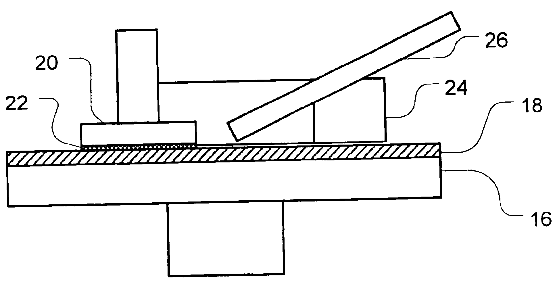
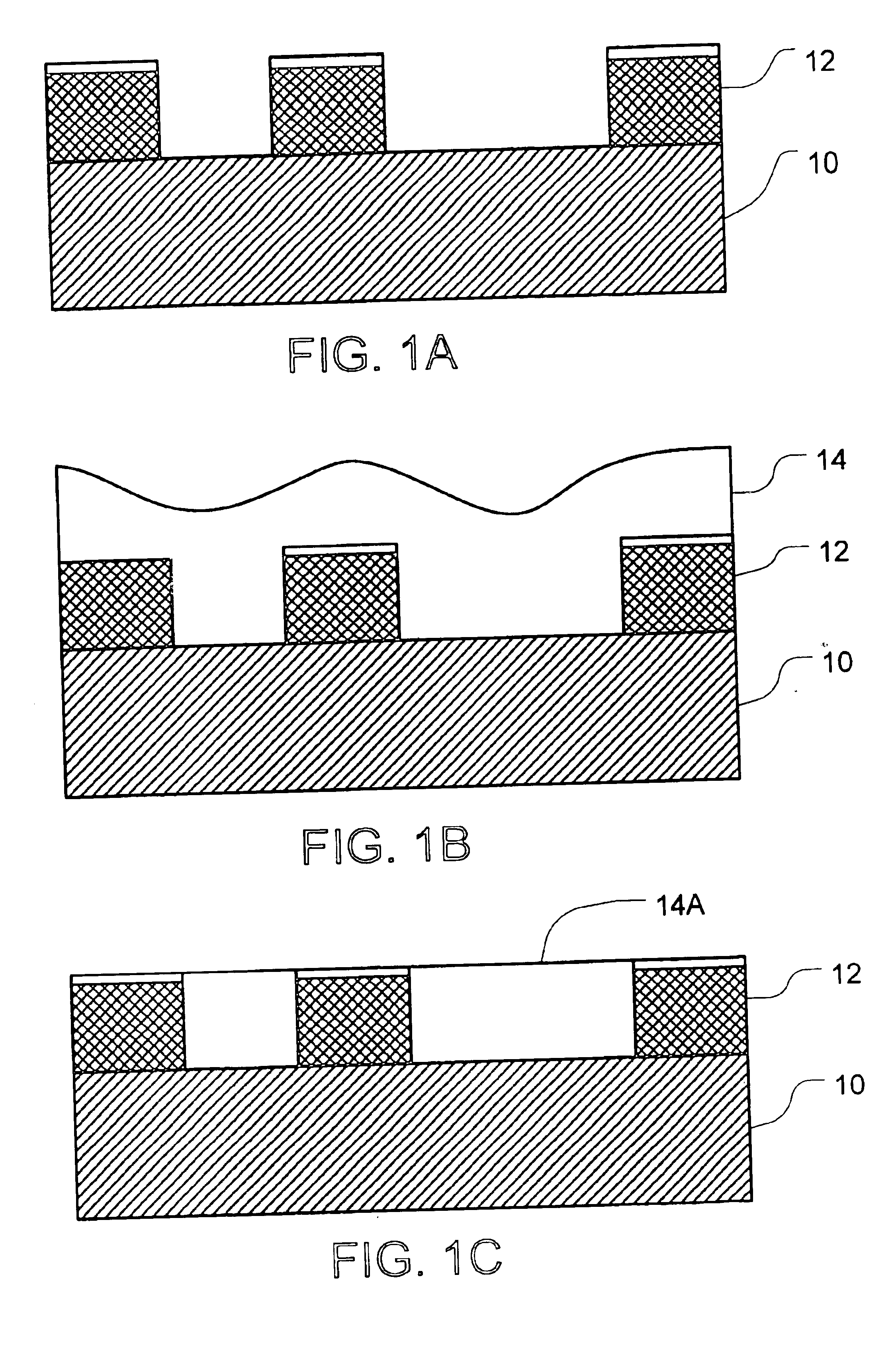
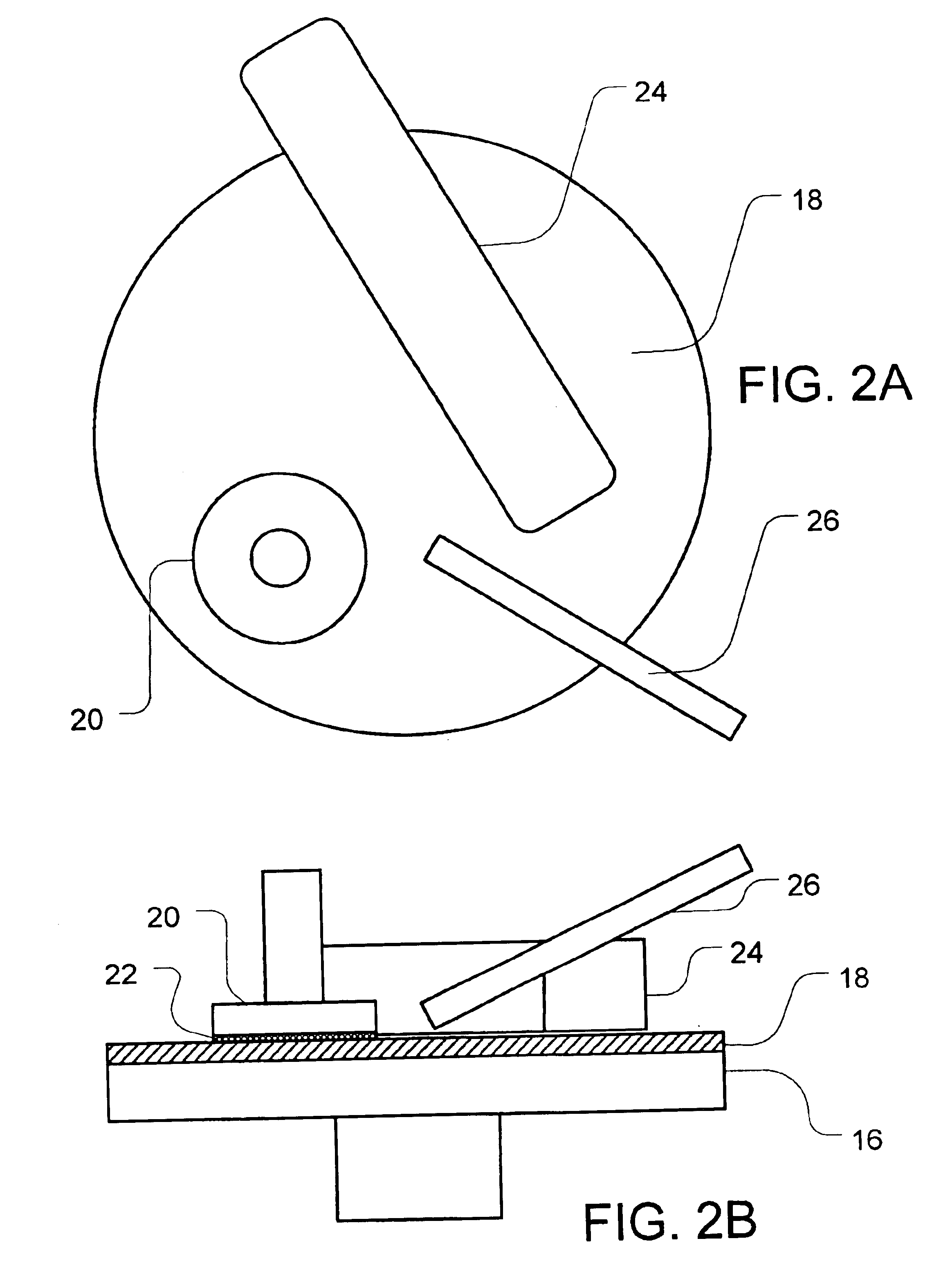
[0032]Described below and illustrated in the accompanying drawings are certain exemplary embodiments according to the invention. These exemplary embodiments are described in sufficient detail to enable those of skill in the art to practice the invention, but are not to be construed as unduly limiting the scope of the following claims. Indeed, those of skill in the art will readily appreciate that other embodiments may be utilized and that process or mechanical changes may be made without departing from the spirit and scope of the inventions as described.

[0033]The present invention provides methods useful in the production of semiconductor devices. As referred to herein, such devices include any wafer, substrate or other structure comprising one or more layers comprising conducting, semiconducting, and insulating materials. The terms wafer and substrate are used herein in their broadest sense and include any base semiconductor structure such as metal-oxide-silicon (MOS), shallow-tren...


PUM

PropertyMeasurementUnit
pressure removal rateaaaaaaaaaa
particle sizeaaaaaaaaaa

Abstract

Provided are materials and methods for the chemical mechanical planarization of material layers using a down force of less than about 2.5 psi while maintaining a material removal rate generally similar to that obtained using higher down forces while simultaneously improving the selectivity of the process with respect to a primary material formed over a barrier material. The materials and methods disclosed herein are suitable for use in meatallization operations during semiconductor device fabrication, in particular in processes in which the primary material is a softer metal such as copper and the barrier material is a harder material such as a metal nitride.

Description

TECHNICAL FIELD[0001]The present invention relates generally to materials and methods for planarizing semiconductor substrates and, in particular, to methods of removing process material layers from the surface of semiconductor substrates using fixed abrasive pads at low pressure and with high selectivity.BACKGROUND[0002]Ultra large scale integrated (ULSI) semiconductor devices, such as dynamic random access memories (DRAMs) and synchronous dynamic random access memories (SDRAMs), consist of multiple layers of conducting, semiconducting, and insulating materials, interconnected within and between layers in specific patterns designed to produce desired electronic functionalities. The materials are selectively patterned on each layer of the device, using lithographic techniques, typically by depositing one or more layers, patterning or masking the layers, and then etching the exposed portions of the materials.[0003]Semiconductor device manufacturing is a very precise process, particul...

Claims


Application Information

Patent Timeline
Patent Type & Authority Patents(United States)
IPC IPC(8): B24B49/16B24B37/04B24B53/007
CPCB24B53/017B24B49/16B24B37/04B24B53/007
Inventor BALIJEPALLI, SUDHAKARALDRICH, DALE J.GRIER, LAURA A.MILLS, MICHAEL E.
Owner DOW GLOBAL TECH LLC
Why Eureka
Try Eureka