

Method for forming TiSiN film, diffusion preventive film comprising TiSiN film, semiconductor device and its production method, and apparatus for forming TiSiN film
a technology of diffusion prevention and film, applied in the direction of semiconductor/solid-state device details, coatings, transistors, etc., can solve the problems of unsatisfactory performance of ti or tin barrier films used in combination with cu wiring lines, prone to migration of copper (cu), similar to aluminum (, ), and easy diffusion at low temperatures
- Summary
- Abstract
- Description
- Claims
- Application Information
AI Technical Summary
Benefits of technology
Problems solved by technology
Method used
Image

Examples
experiment 1
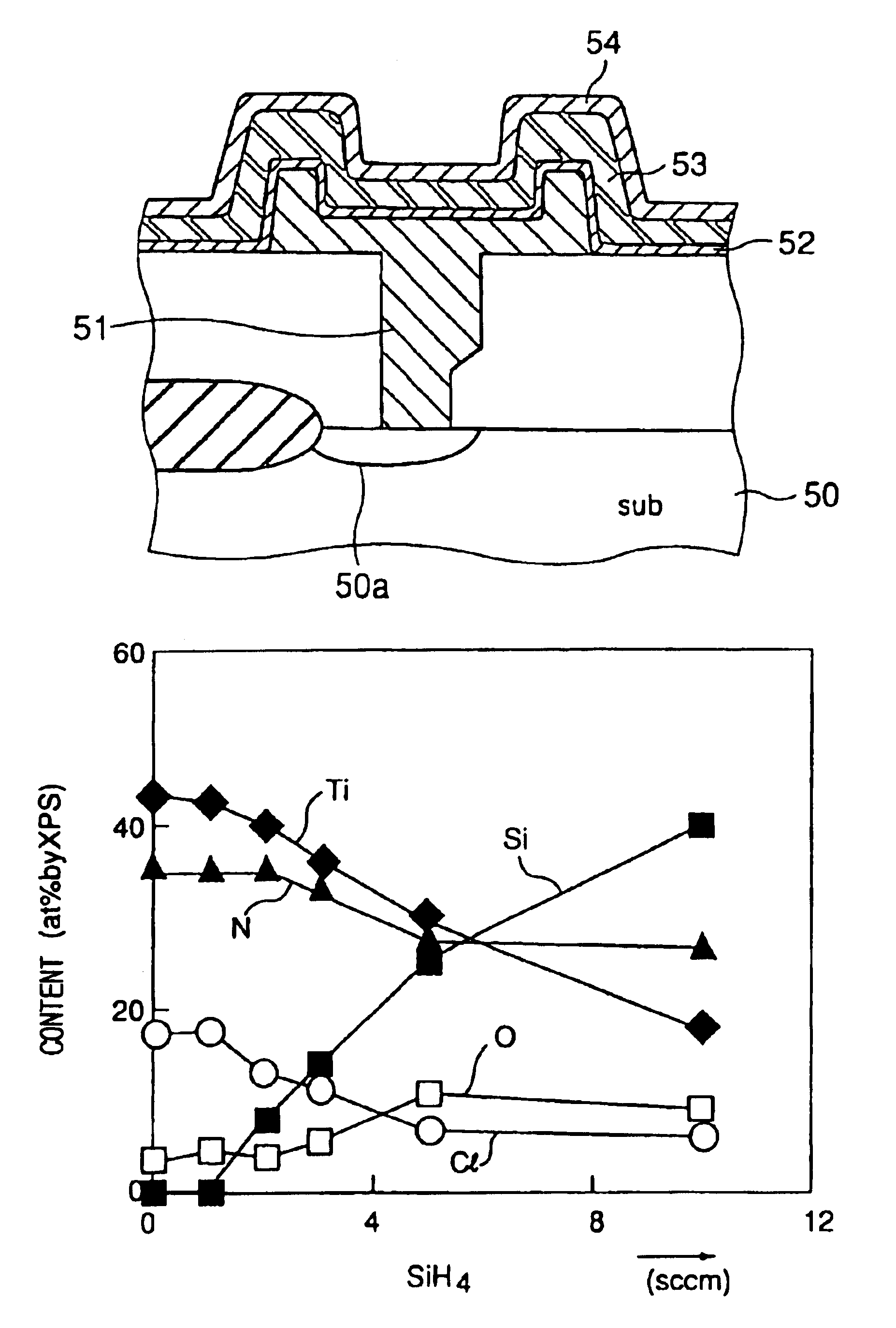
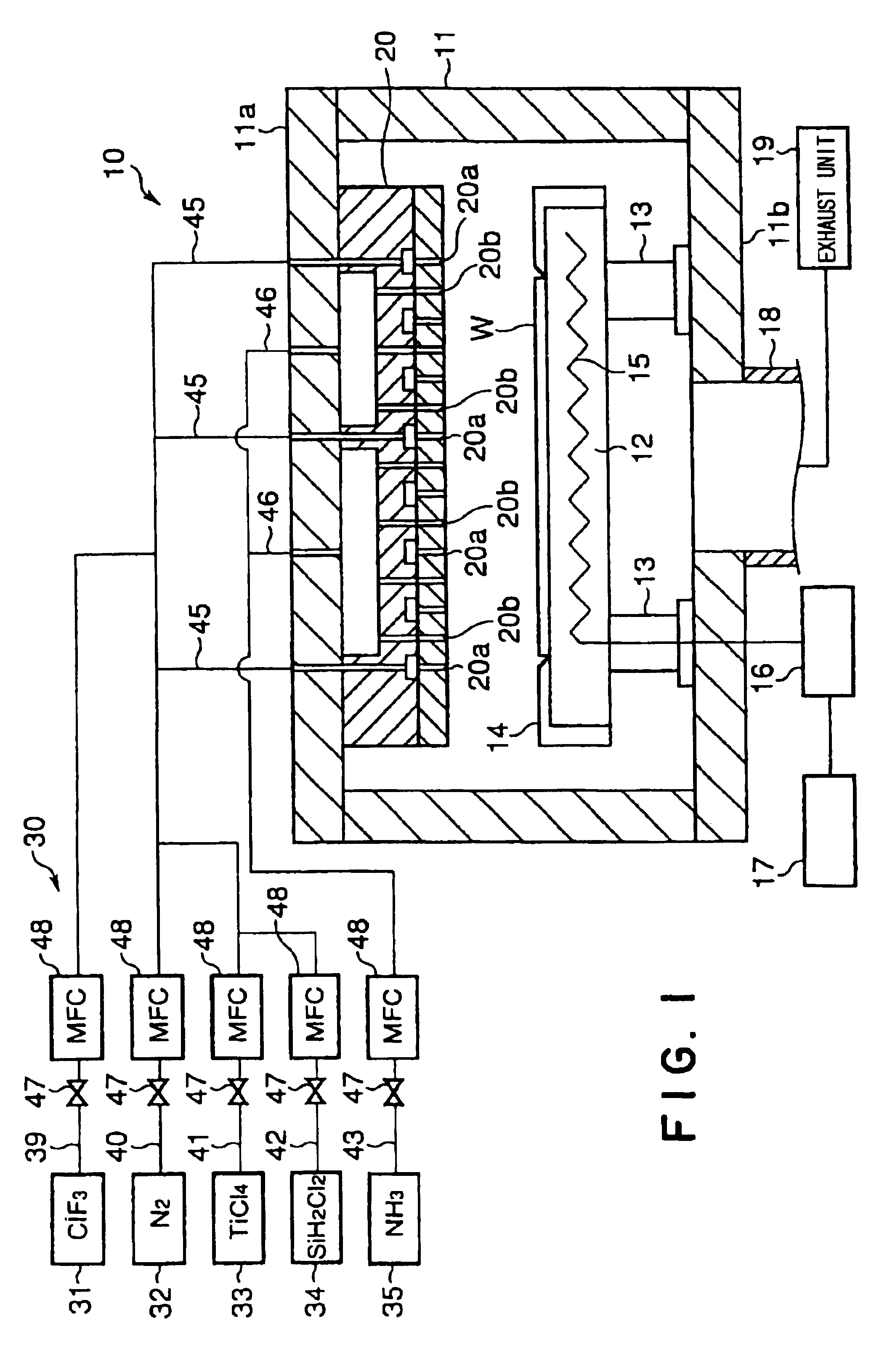
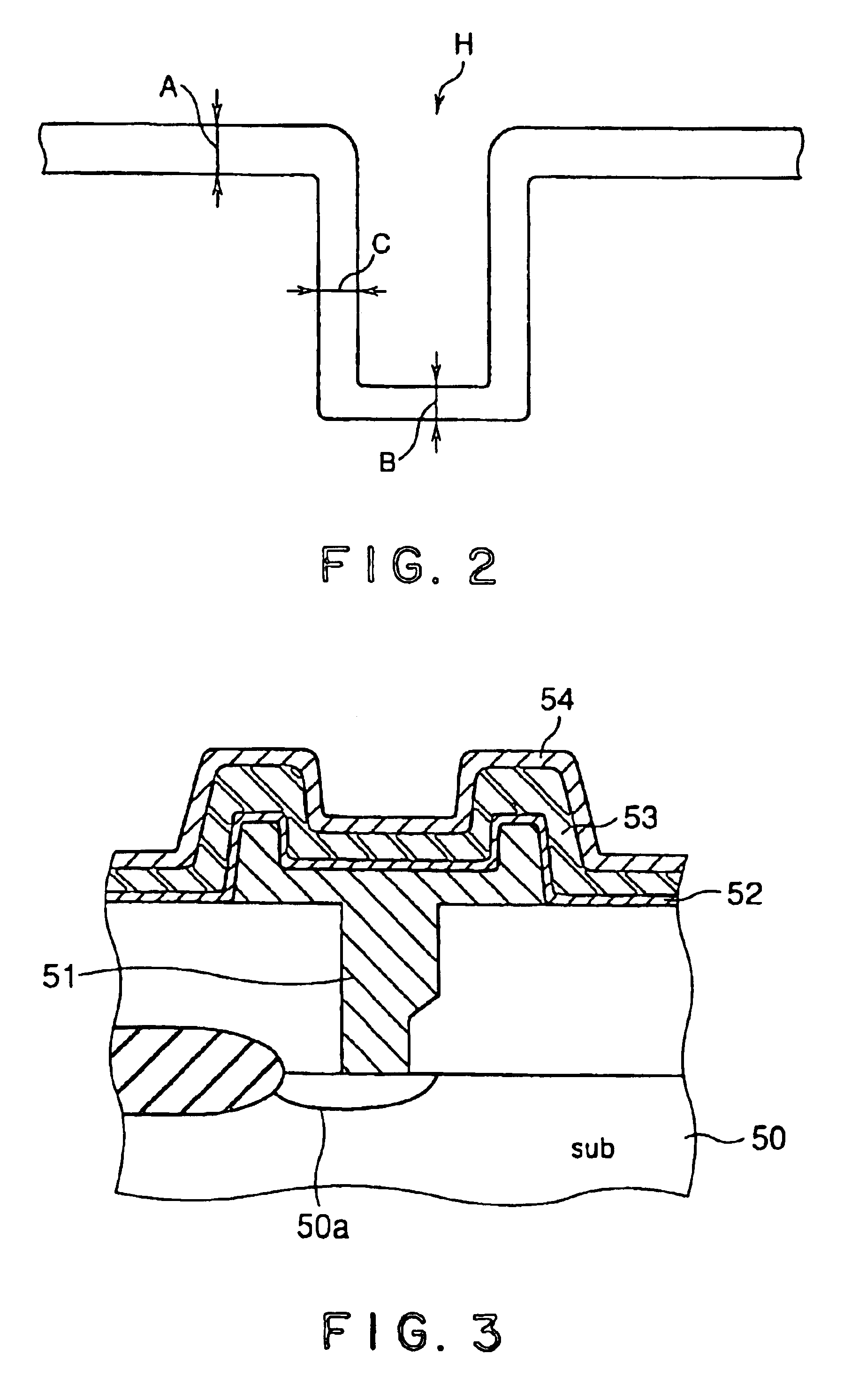
[0145]TiSiN film forming experiments were conducted under the following process conditions (film-deposition conditions).[0146]Wafer temperature: 400° C. (Fixed)[0147]Pressure: 1 Torr, 3 Torr[0148]Flow rate of TiCl4 gas: 10 sccm (Fixed)[0149]Flow rate of H2 gas: 1000 sccm, 2000 sccm[0150]Flow rate of Ar gas: 100 sccm, 500 sccm, 1000 sccm[0151]Flow rate of N2 gas: 100 sccm, 2000 sccm, 500 sccm[0152]Flow rate of SiH4 gas: 0 sccm, 1 sccm, 2 sccm, 5 sccm[0153]Radio-frequency power: 200 W, 500 W[0154]Frequency of radio-frequency power: 13.56 MHz (Fixed)
[0155]The following are suitable process conditions for forming a TiSiN film satisfactory in Cl-content and resistivity selected from the foregoing process conditions.[0156]Wafer temperature: 400° C.[0157]Pressure: 3 Torr[0158]Flow rate of TiCl4 gas: 10 sccm[0159]Flow rate of H2 gas: 2000 sccm[0160]Flow rate of Ar gas: 100 sccm[0161]Flow rate of N2 gas: 500 sccm[0162]Flow rate of SiH4 gas: 5 sccm[0163]Radio-frequency power: 500 W[0164]Frequ...
experiment 2
[0177]Experiment was conducted to form a plurality of types of TiSiN films respectively having different compositions by changing process conditions as shown below and to evaluate the heat-resistance of the TiSiN films. Each test sample was prepared by forming a TiSiN film on a Si wafer, and forming a Cu film on the TiSiN film.
Process Conditions 2-a (Identical to the Foregoing STD Conditions)
[0178]Wafer temperature: 400° C.[0179]Process pressure: 3 Torr[0180]Flow rate of TiCl4 gas: 10 sccm[0181]Flow rate of H2 gas: 2000 sccm[0182]Flow rate of Ar gas: 100 sccm[0183]Flow rate of N2 gas: 500 sccm[0184]Flow rate of SiH4 gas: 5 sccm[0185]Frequency of radio-frequency power: 13.56 MHz[0186]Radio-frequency power: 500 W
[0187]Process conditions 2-b were the same as the process conditions 2-a, except that the flow rate of SiH4 gas was 3 sccm.
[0188]Process conditions 2-c were the same as the process conditions 2-a, except that the flow rate of SiH4 ...
experiment 3
[0192]Experiments were conducted under the following process conditions to confirm the effect of radio-frequency power of 60 MHz on the compositions of TiSiN films.
Process Conditions 3-a
[0193]Process conditions 3-a were the same as the process conditions 2-a (STD), except that radio-frequency power of 60 MHz was used.
Process Conditions 3-b
[0194]Process conditions 3-b were the same as the process conditions 2-a (STD), except that the process pressure was 1 Torr, the flow rate of SiH4 gas was 7 sccm and radio-frequency power of 60 MHz was used.
[0195]The respective compositions of TiSiN films formed under those process conditions are shown in Table 2
[0196]
TABLE 2ProcessComposition (atomic percent), (at %)conditionsTiSiNCl3-a18.921.332.220.53-b38.710.533.312.2
[0197]The film formed under the process conditions 3-a, which differs from the standard process conditions 2-a only in the frequency of the radio-frequency power, had a high resistance (80,200 μΩ·cm) and was found to be unsuitabl...
PUM
| Property | Measurement | Unit |
|---|---|---|
| Temperature | aaaaa | aaaaa |
| Pressure | aaaaa | aaaaa |
| Power | aaaaa | aaaaa |
Abstract
Description
Claims
Application Information