Dual (constant voltage/constant current) bias supply for linear power amplifiers

a power amplifier and constant current technology, applied in the field of linear rf power amplifier bias networks, can solve the problems of high internal impedance, resistor b, circuit is very sensitive to vref and requires high accuracy/higher cost voltage regulators

Active Publication Date: 2005-07-26
CALLAHAN CELLULAR L L C
View PDF6 Cites 66 Cited by
  • Summary
  • Abstract
  • Description
  • Claims
  • Application Information

AI Technical Summary

Problems solved by technology

The main problem with this style of bias supply is its high internal impedance, a resistor 102 when applied to non-constant envelope modulation schemes (e.g., CDMA, W-CDMA, and QPSK).
With a lower base voltage the RF power transistor collector current cannot follow the AM (+3 dB) component of the modulation and distortion results.
Two issues remain for this type of bias; first, the inclusion of the pass transistor reduces the temperature tracking accuracy of the current

Method used


Image

  • Dual (constant voltage/constant current) bias supply for linear power amplifiers
  • Dual (constant voltage/constant current) bias supply for linear power amplifiers
  • Dual (constant voltage/constant current) bias supply for linear power amplifiers

Examples


Embodiment Construction

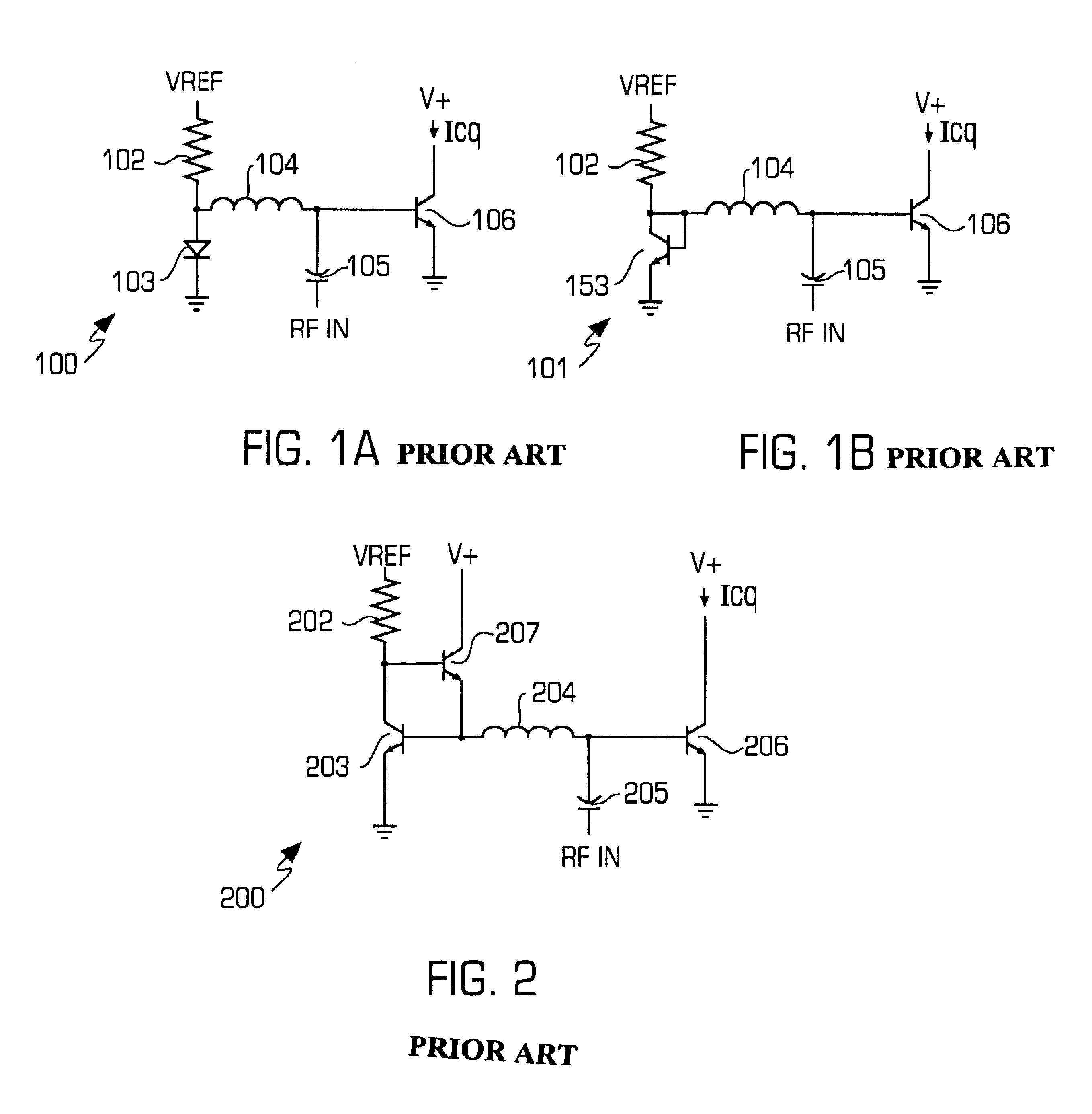
[0013]FIGS. 1A and 1B are schematic diagrams illustrating conventional power amplifiers 100 and 101, respectively, that include respective diode bias and current mirror circuits for nonlinear amplifiers having a constant envelope.

[0014]The power amplifier 100 comprises a diode bias circuit including a resistor 102 and a diode 103 serially connected to bias a radio frequency (RF) transistor 106. A capacitor 104 is an RF coupling capacitor of an RF signal from a previous stage and functions as a DC block for the bias supply. An inductor 104 functions as a large impedance to inhibit any RF from the bias supply.

[0015]The power amplifier 101 comprises a current mirror circuit including a resistor 102 and a transistor 153 serially connected to bias the RF transistor 106.

[0016]The power amplifiers 100 and 101 track temperature well because the referenced diode junctions of the diode 103 and the transistor 153 are on the same die as the RF device (transistor 106). The amplifiers 100 and 101...


PUM


Abstract

An RF amplifier comprises a power amplifier and a dual bias circuit. A dual bias circuit comprises a constant current source and a constant voltage source for biasing the power amplifier. The power may include a heterojunction bipolar transistor (HBT) or a bipolar junction transistor (BJT).

Description

[0001]This application claims the benefit of U.S. Provisional Application No. 60 / 436,037, filed Dec. 23, 2002.BACKGROUND[0002]The invention relates to a linear (e.g., CDMA) RF power amplifier bias networks, and more particularly to a linear RF power amplifier including a dual bias supply for maintaining a constant quiescent operating bias point over temperature and a range of control voltages.[0003]For constant envelope bipolar transistor based power amplifiers (GSM, FM) generally all that is required of a bias network is to set the bias point for the class of operation desired, and to track the base voltage with temperature to maintain a stable operating point. This is easily obtained with a passive bias scheme (current Mirror / constant current CC) as shown in FIG. 1, described below. The “on chip” diode or the diode connected transistor track the RF power device base voltage very well whether implemented in silicon or the lower thermally conductive GaAs substrates. Also with this a...

Claims


Application Information

Patent Timeline
IPC IPC(8): H03F1/30H03F1/32H03F3/189
CPCH03F1/302H03F1/32H03F3/189H03F2200/18H03F2200/451
Inventor GREEN, RON
Owner CALLAHAN CELLULAR L L C
Why Eureka
Try Eureka