Active balun circuit for single-ended to differential RF signal conversion with enhanced common-mode rejection

a technology of active balun and common-mode rejection, which is applied in the field of integrated circuits and subsystems, can solve the problems of affecting signal balance, increasing parasitic capacitance, and limited dynamic range of active balun, and achieves enhanced common-mode rejection, enhanced common-mode rejection, and high linearity

Inactive Publication Date: 2005-07-26
WSOU INVESTMENTS LLC +1
View PDF3 Cites 29 Cited by
  • Summary
  • Abstract
  • Description
  • Claims
  • Application Information

AI Technical Summary

Benefits of technology

[0007]The present invention provides an active balun circuit for single-ended to differential RF signal conversion with enhanced common-mode rejection. The circuit includes a differential pair amplifier with single-ended input and balanced output. The circuit achieves a balanced output via an output network which behaves as an impedance matching network for a differential mode signal and is grounded for a common mode signal. As a result, the common mode signal is suppressed and 180-degree phase balance at output is achieved.
[0008]The circuit further includes a parallel inductor-capacitor (LC) band stop resonator between an emitter-coupled node and a current source that has a very large impedance looking into the current source at the emitter-coupled node, so that the output signal balance is not affected and additional DC voltage drop is not created.
[0009]Advantageously, the active balun circuit for single-ended to differential RF signal conversion with enhanced common-mode rejection of the present invention suppresses common mode signal and achieves phase and amplitude balance without sophisticated tuning or compensation methods. Further the circuit of the present invention achieves high linearity and low residual phase noise simultaneously.

Problems solved by technology

The challenge is to maintain its phase and amplitude balance at high frequency when parasitic effects degrade its performance.
If these interference signals or harmonics enter the mixer, they may create higher order intermodulation products that can block the wanted signal.
On the other hand, an active balun has limited dynamic range when compared to its passive counterpart.
This increases its parasitic capacitance and affects signal balance due to common-mode leakage or signal at high frequency.

Method used


Image

  • Active balun circuit for single-ended to differential RF signal conversion with enhanced common-mode rejection
  • Active balun circuit for single-ended to differential RF signal conversion with enhanced common-mode rejection

Examples


Embodiment Construction

I. Description of the Circuit

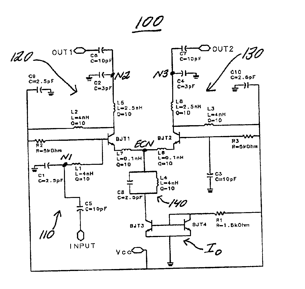
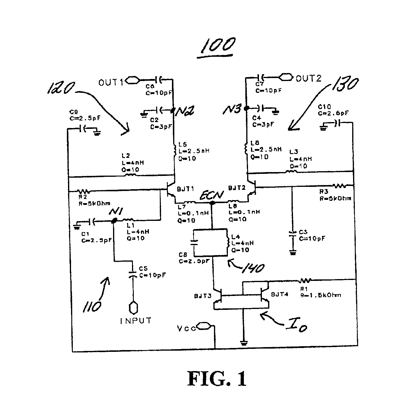
[0012]FIG. 1 is a circuit schematic of the circuit according to the present invention. The circuit is designated generally by reference numeral 100. It is a differential pair amplifier with single-ended input and balanced output.

[0013]The circuit 100 includes a parallel inductor-capacitor (LC) band stop resonator 140 between the emitter-coupled node ECN and the current source Io. The LC band stop resonator 140 includes a capacitor C8 connected in parallel with an inductor L4 which filter out the unwanted parasitic parameters, e.g., parasitic capacitance or oscillations, at RF frequency. A first terminal of the LC band stop resonator 140 is connected to the emitter-coupled node ECN and a second terminal of the LC band stop resonator 140 is connected to a collector of the transistor BJT3. A first terminal of a resistor R1 is connected to the base of the transistors BJT3, BJT4 and a collector of the transistor BJT4. A second terminal of the resistor R1 is c...


PUM


Abstract

An active balun circuit is provided for single-ended to differential RF signal conversion with enhanced common-mode rejection which suppresses common mode signal and which achieves phase and amplitude balance without sophisticated tuning or compensation methods. The circuit has a single-ended input and balanced output with phase and amplitude balance error less than 2° and 1.2 dB, respectively, measured from 1.5 GHz to 1.8 GHz at 5V supply. When supply voltage drops down to 1.5V, its phase and amplitude balance error remains within 5° and 2 dB, respectively. The circuit achieves a balanced output via an output network which behaves as an impedance matching network for differential mode signal and is grounded for common mode signal. As a result, common mode signal is suppressed and 180-degree phase balance at output is achieved. The circuit has high-linearity (P1 dBin=5 dBm, IIP3=16.6 dBm) and low residual phase noise (<−155 dBc / Hz at 100 kHz and above) which make it suitable as an active balun / buffer amplifier between LO and balanced mixer for base station receiver applications.

Description

BACKGROUND OF THE INVENTION[0001]1. Field of the Invention[0002]The present invention relates generally to the field of integrated circuits and subsystems. Specifically, the present invention relates to an active balun circuit for single-ended to differential RF signal conversion with enhanced common-mode rejection.[0003]2. Description of the Related Art[0004]A differential-pair amplifier can be used in integrated circuits as an active balun when single-ended to differential conversion is needed, e.g., the radio-frequency (RF) and local oscillator (LO) ports of balanced mixers. The challenge is to maintain its phase and amplitude balance at high frequency when parasitic effects degrade its performance. Several techniques have been reported to improve the phase and amplitude balance as well as the bandwidth.[0005]However, for integrated circuits used in wireless communications, narrow band response is a preferred feature because it helps reject unwanted signals. For example, a narrow...

Claims


Application Information

Patent Timeline
Patent Type & Authority Patents(United States)
IPC IPC(8): H03H11/02H03H11/32
CPCH03H11/32
Inventor LIN, JENSHAN
Owner WSOU INVESTMENTS LLC
Why Eureka
Try Eureka