Light emitting device using LED

a technology of light emitting devices and led light, which is applied in the direction of semiconductor devices, basic electric elements, electrical equipment, etc., can solve the problems of inability to provide efficient light reflection, inefficiency of light extraction, and inability to efficiently extract light, so as to improve the efficiency of light extraction and efficient reflect light

Inactive Publication Date: 2005-08-16
SATCO PRODS
View PDF12 Cites 128 Cited by
  • Summary
  • Abstract
  • Description
  • Claims
  • Application Information

AI Technical Summary

Benefits of technology

[0014]In this structure, the light emitting diode chip is placed on the bottom of the housing recess that is a part of the metal plate so as to be thermally coupled to the metal plate. Therefore, the heat radiation can be enhanced as compared to a conventional device where a chip is mounted through the insulating layer. This can protect the light emitting diode chip from temperature rise that may cause decrease of the luminous efficiency, decrease of the operating life, and deterioration of the sealing resin. The inner surface of the housing recess, which is a part of the metal plate, functions as a light reflector so that light emanated from the light emitting diode chip can be reflected on the inner surface of the housing recess for extraction out of the housing recess. Thus, the light extraction efficiency can be increased. Since the light reflector is made of metal, not resin, it can be prevented from decrease in the reflecting ability due to heating in mounting process of the light emitting diode chip or due to exposure to light from the light emitting diode chip in making the device in use.
[0024]In the improved light emitting device, preferably, the insulating substrate has a portion on which the metal plate is not layered, the portion of the insulating substrate having a back at which circuit components are mounted. This allows even a lead-mount circuit component to be mounted without the risk of a short-circuit via the metal plate. Further, since light emitted from the light emitting diode chip is prevented from being absorbed in or reflected on the circuit component, the light can be extracted to the outside further efficiently.

Problems solved by technology

Additionally, the conventional light emitting device has the following disadvantage in the efficiency of light extraction from the LED chip 1.
If the LED chip 1 is positioned deeper than the region of the round hole in the frame member 30 where the radius is the smallest, light from the LED chip 1 is partially blocked, thus failing to be extracted efficiently.
1. Thus, efficient reflection of light cannot be provided.
Therefore, the conventional light emitting device is disadvantageous in that light emitted sideward from the LED chip 1 fails to be efficiently extracted to the outside.
However, when heated in mounting process of the LED chip 1, the white resin may be oxidized to be colored, thus decreased in the reflecting ability.

Method used


Image

  • Light emitting device using LED
  • Light emitting device using LED
  • Light emitting device using LED

Examples


embodiment 1

(Embodiment 1)

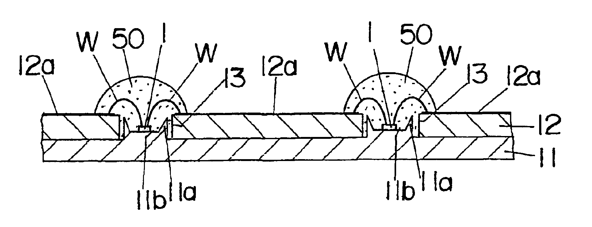
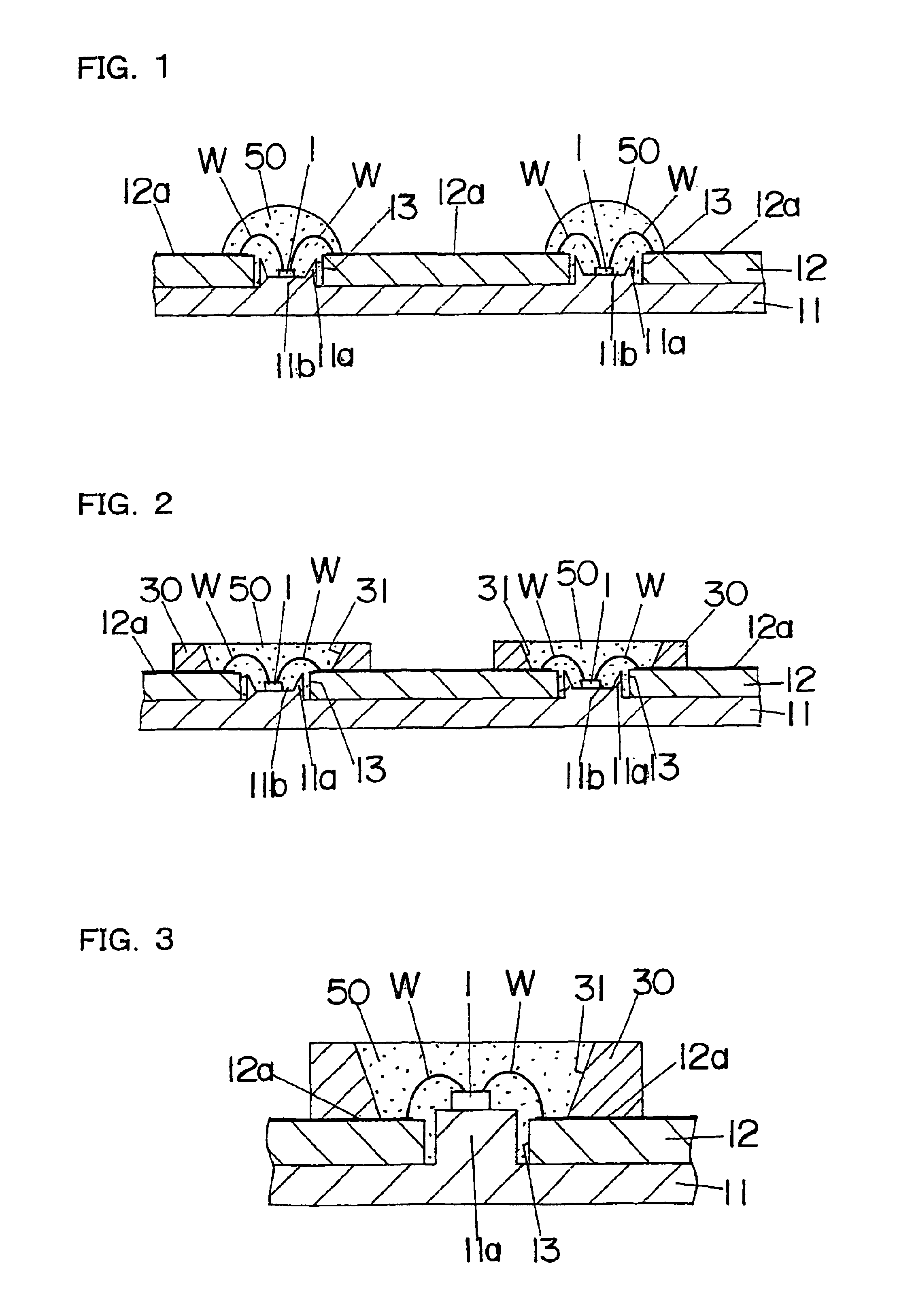
[0046]As shown in FIG. 1, a light emitting device according to this embodiment includes a metal plate 11 that is made of aluminum and has a plurality of cylindrical projections 11a each projecting forward (upward in FIG. 1) and a printed circuit board 12 that has a grass epoxy substrate as the insulating substrate and is joined, in layers, to the front surface of the metal plate 11. Each of the projections 11a has a front side provided with a housing recess 11b, in which a light emitting diode chip (hereinafter, referred to as an LED chip) 1 is accommodated. The LED chip 1 is encapsulated in a transparent resin seal portion 50, together with a bonding wire W, which will be described below.

[0047]The housing recess 11b formed in the metal plate 11 is sized so that the LED chip 1 is mounted directly on the bottom of the recess while the depth of the recess is larger than the thickness of the LED chip 1.

[0048]The LED chip 1 is mounted (disposed) in a state where it is ther...

embodiment 2

(Embodiment 2)

[0058]As shown in FIG. 2, a light emitting device according to this embodiment includes a frame member 30 in addition to the components included in the light emitting device according to Embodiment 1. By adding this member, the configuration of a resin seal portion 50 is modified. Since the light emitting device according to this embodiment is substantially identical in basic structure to the device according to Embodiment 1, like components are denoted by like numerals and will be explained in no more detail.

[0059]The frame member 30 is made of a white plastic resin and configured like a frame (circular). The frame member is joined to the front surface of the printed circuit board 12 so as to surround the insertion hole 13. Sealing resin, which forms the resin seal portion 50, is poured into the frame member 30 for encapsulation of an LED chip 1 and a bonding wire W. The front surface of the resin seal portion 50 and the front surface of the frame member 30 are arrang...

embodiment 3

(Embodiment 3)

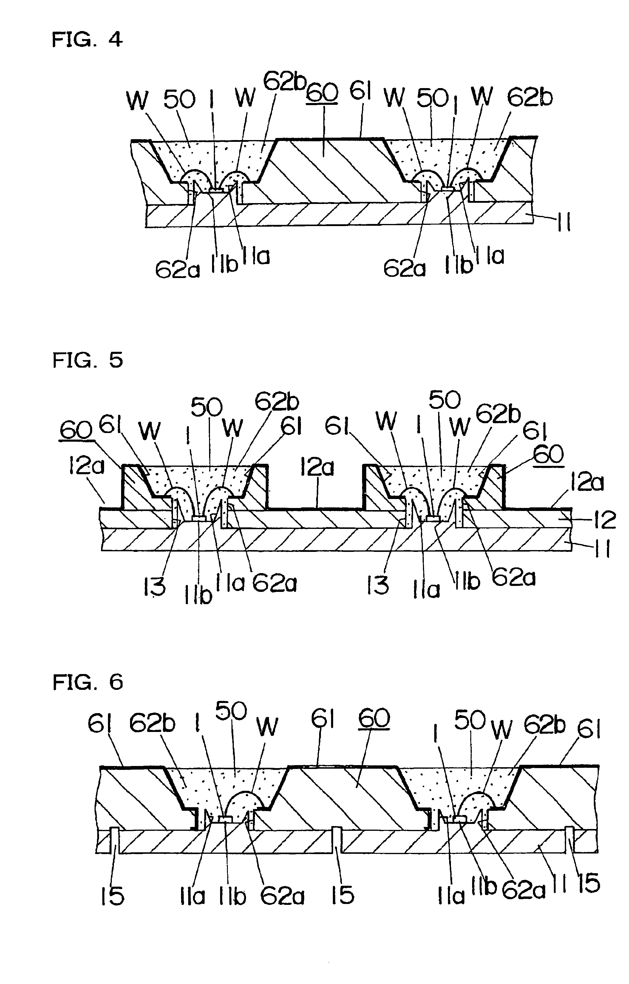
[0064]As shown in FIG. 4, a light emitting device according to this embodiment includes a MID (Molded Interconnected Device) substrate 60 (three-dimensional molded circuit board) that has a resin insulating substrate molded to be non-planar and a wiring portion 61 provided in three dimensions on the surfaces of the insulating substrate, in place of the printed circuit board 12 described in Embodiment 1. Like components as those of Embodiment 1 are denoted by like numerals and will be explained in no more detail.

[0065]The MID substrate 60 is joined to the front surface of a metal plate 11. The MID substrate 60 has an insertion hole 62a into which a projection 11a projecting forward from the front surface of the metal plate 11 is inserted and a hole as a resin filled portion 62b that is communicated with the insertion hole 62a and is larger in inside diameter than the insertion hole 62a. The inside diameter of the resin filled portion increases toward the opening. The in...


PUM


Abstract

A light emitting device that can provide enhanced heat radiation as well as allowing light from a light emitting diode (LED) chip to be efficiently extracted out of the device. This light emitting device includes a metal plate (11) that is made of aluminum. The metal plate (11) has a projection (11a) projecting forward. The projection (11a) has a front side provided with a housing recess (11b). An LED chip (1) is mounted on the bottom of the housing recess (11b) so that it is thermally coupled to the metal plate (11), thus allowing heat to be radiated efficiently. A printed circuit board (12), having a grass epoxy substrate to be joined to the front surface of the metal plate (11), is provided with an insertion hole (13) into which the projection (11a) is inserted. The LED chip (1) and a bonding wire (W) are encapsulated in a transparent resin seal portion (50). The side wall of the housing recess (11b) that is part of the metal plate (11) functions as a reflector for reflecting forward light emitted from the LED chip (1). Thus, light from the LED chip (1) can be extracted efficiently.

Description

TECHNICAL FIELD[0001]The present invention relates to light emitting devices using light emitting diode (LED) chips.BACKGROUND ART[0002]A light emitting device using a light emitting diode chip has been conventionally proposed that is shown in FIGS. 18A and 18B. In the conventional device, the light emitting diode chip (hereinafter, referred to as LED chip) 1 is mounted on a metal mounting board 20 that includes a metal plate 21 made of a metal with a high thermal conductivity, e.g. aluminum, an insulating layer 22 made of an insulating resin material, e.g. glass epoxy and provided on a surface of the metal plate, and a wiring portion (wiring pattern) 23 that is a copper foil provided on the insulating layer 22.[0003]The LED chip 1 is electrically connected with the wiring portion 23 through a bonding wire W. The LED chip 1 includes, for example, a sappshire substrate and a gallium nitride light emitting portion provided on the sapphire substrate.[0004]The conventional light emittin...

Claims


Application Information

Patent Timeline
Patent Type & Authority Patents(United States)
IPC IPC(8): H01L33/00H01L25/075H01L33/64H01L33/32H01L33/54H01L33/60
CPCH01L33/642H01L25/0753H01L25/167H01L2224/45144H01L2924/00014H01L2224/48227H01L2224/48091H01L2924/181H01L2924/00012
Inventor HASHIMOTO, TAKUMASUGIMOTO, MASARUKIMURA, HIDEYOSHISHIOHAMA, EIJI
Owner SATCO PRODS
Why Eureka
Try Eureka