
Multi-layered unit

a multi-layer unit and multi-layer technology, applied in the direction of multiple fixed capacitors, fixed capacitor details, capacitors, etc., can solve the problems of high probability of power supply noise, low impedance required of power supply wiring, and lsi operation erroneously, etc., to achieve excellent dielectric characteristics, small size, and large capacitance

Inactive Publication Date: 2005-08-16
TDK CORPARATION
View PDF20 Cites 33 Cited by
  • Summary
  • Abstract
  • Description
  • Claims
  • Application Information

AI Technical Summary

Benefits of technology

[0017]It is therefore an object of the present invention to provide a multi-layered unit suitable for fabricating a thin film capacitor having a small size, large capacitance and an excellent dielectric characteristic and suitable for fabricating an inorganic EL (electro-luminescence) device capable of emitting light having high luminescence.

Problems solved by technology

In the LSI having a high operating frequency, power supply noise is very likely to be generated, and once power supply noise occurs, a voltage drop occurs due to parasitic resistance and parasitic inductance of the power supply wiring, causing the LSI to operate erroneously.
Therefore, in current LSIs, which have high integration density, low operating voltage and high operating frequency, the impedance required of the power supply wiring is extremely low.
However, since the size of an electrolytic capacitor or multilayer ceramic capacitor is relatively large, it is difficult to integrate it with an LSI.
Therefore, the electrolytic capacitor or multilayer ceramic capacitor has to be mounted on a circuit substrate independently of the LSI and, as a result, the length of wiring for connecting the terminals of the LSI power supply and the decoupling capacitor is inevitably long.
Accordingly, in the case where an electrolytic capacitor or a multilayer ceramic capacitor is employed as a decoupling capacitor, it is difficult to lower the inductance of the wiring for connecting the terminals of the LSI power supply and the decoupling capacitor.
However, the thin film capacitor employing any one of the above mentioned materials is disadvantageous in that the temperature characteristic thereof is poor.
For example, since the dielectric constant of BST has a temperature dependency of −1000 to −4000 ppm / ° C., in the case where BST is employed as a dielectric material, the capacitance of the thin film capacitor at 80° C. varies between −6% and −24% in comparison with that at 20° C. Therefore, a thin film capacitor employing BST as a dielectric material is not suitable for use as a decoupling capacitor for a high operating frequency LSI whose ambient temperature frequently reaches 80° C. or higher owing to heat generated by electric power consumption.
Therefore, in the case where any one of the above mentioned materials is used as a dielectric material for a thin film capacitor, it is difficult to simultaneously make the thin film capacitor small and the capacitance thereof great.
The property of the bismuth layer structured compound as a ferroelectric material is undesirable when the bismuth layer structured compound is utilized as a dielectric material for a thin film capacitor since it causes variation in dielectric constant.

Method used


Image

  • Multi-layered unit
  • Multi-layered unit
  • Multi-layered unit

Examples


Embodiment Construction

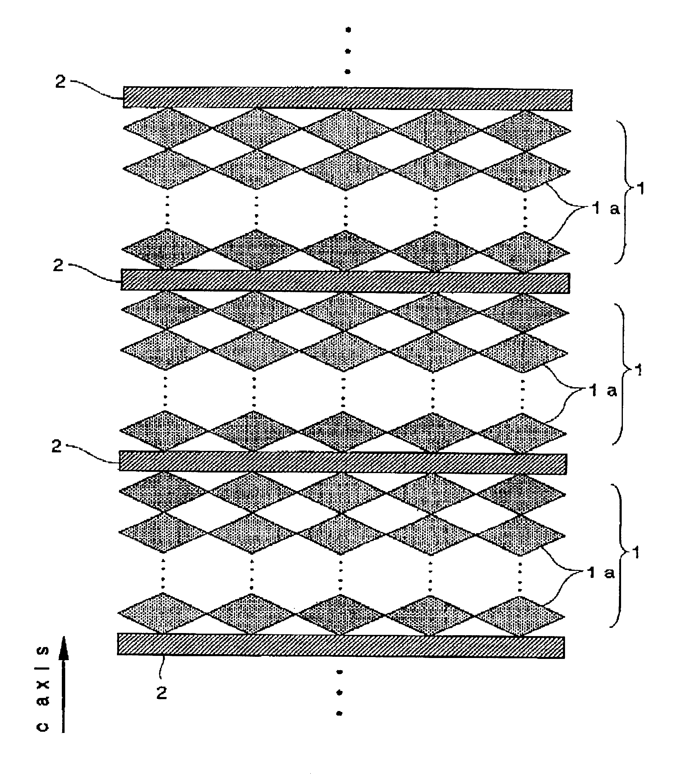
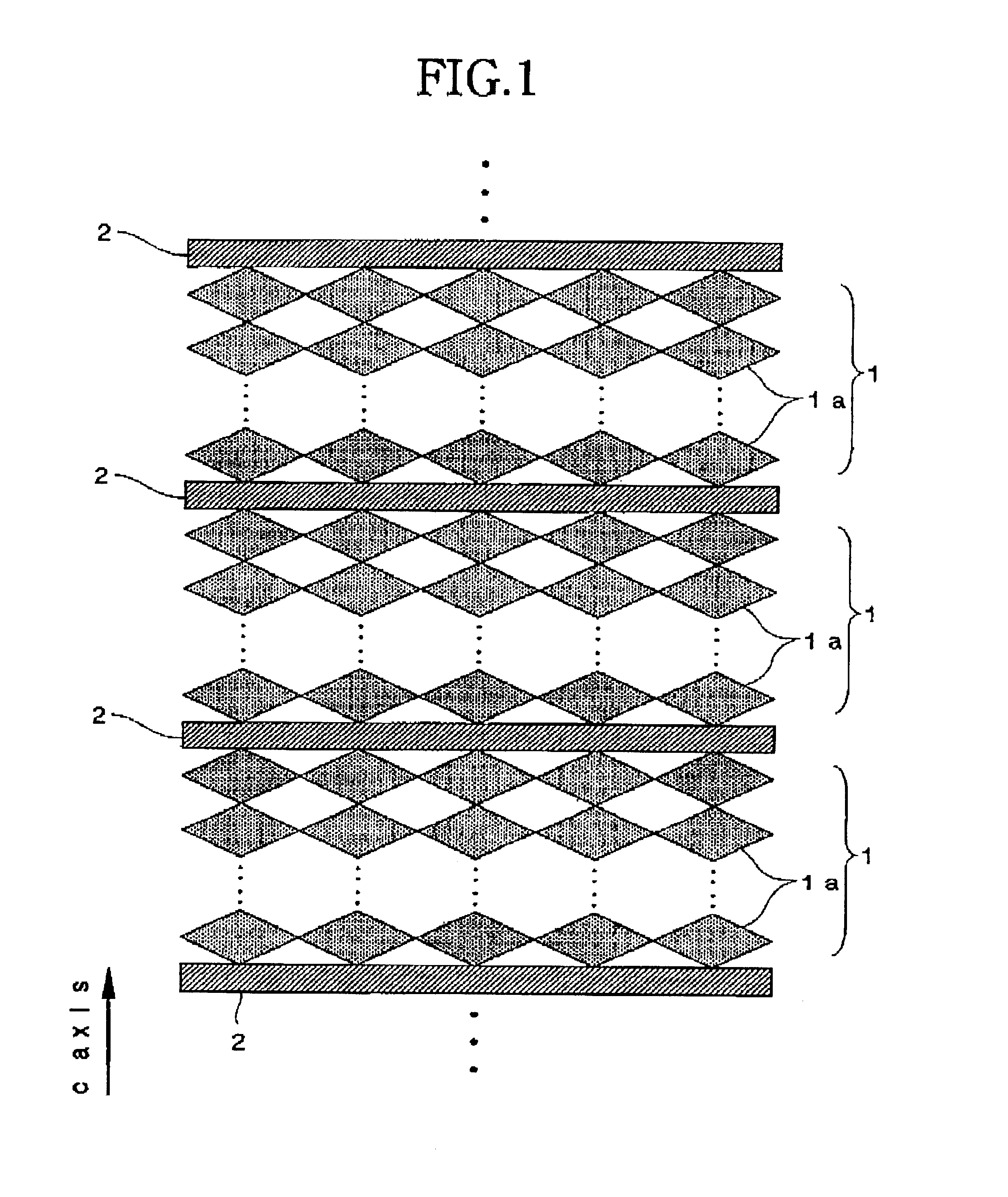
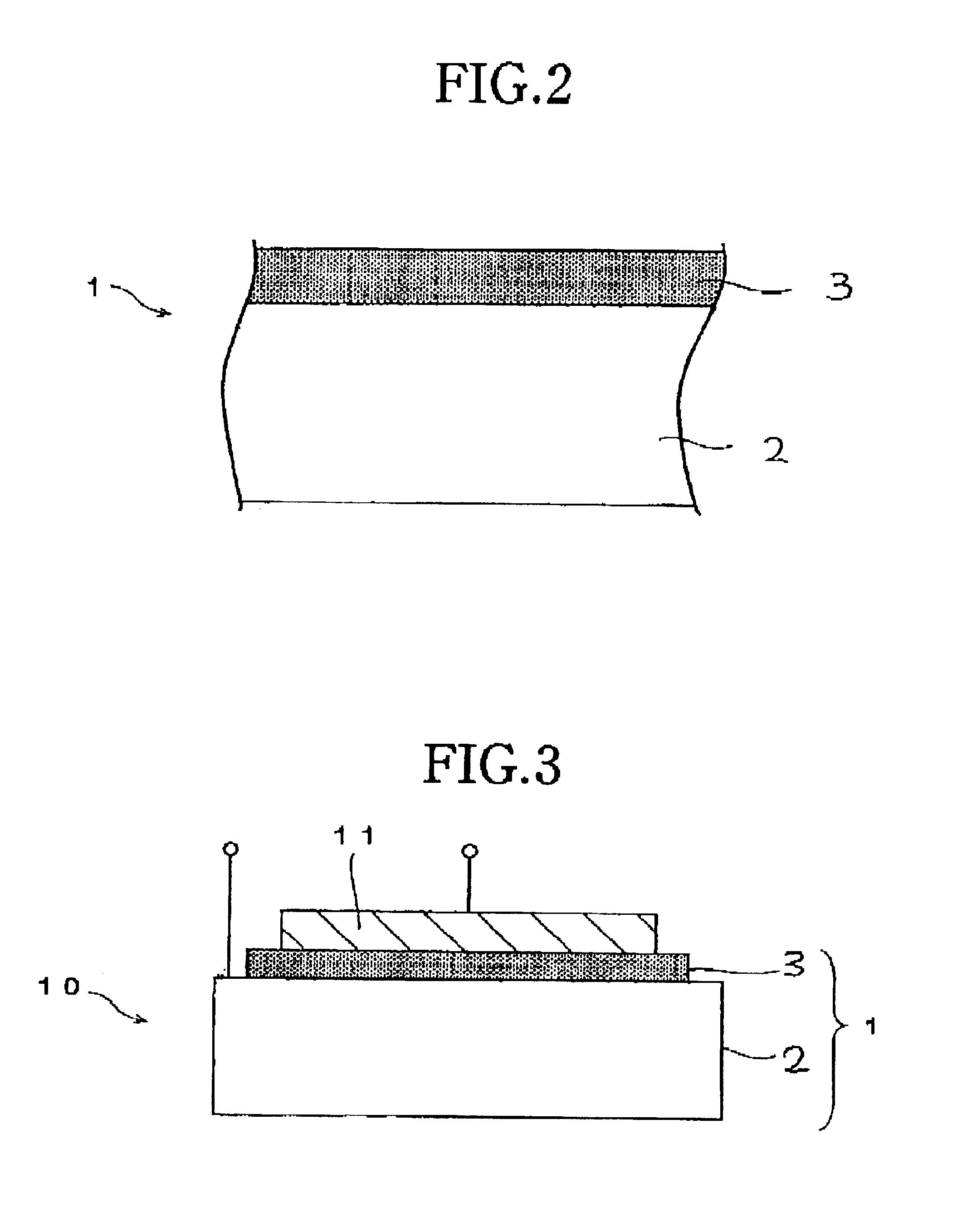
[0060]FIG. 2 is a schematic partial cross-sectional view showing a multi-layered unit which is a preferred embodiment of the present invention.

[0061]As shown in FIG. 2, a multi-layered unit 1 according to this embodiment includes a dielectric layer 3 on a support substrate 2.

[0062]In this embodiment, the support substrate 2 of the multi-layered unit 1 is formed of platinum (Pt) and oriented in the [001] direction.

[0063]Therefore, the support substrate 2 serves not only as a support for mechanically supporting the multi-layered unit 1 but also as an electrode layer.

[0064]Further, since the support substrate 2 is formed of platinum (Pt) and oriented in the [001] direction, the support substrate 2 serves as an electrode layer and a buffer layer for ensuring that a dielectric layer 3 containing a bismuth layer structured compound oriented in the [001] direction, namely, the c axis direction, can be formed by epitaxially growing a dielectric material containing the bismuth layer structur...


PUM


Abstract

A multi-layered unit according to the present invention includes a support substrate formed of a material which has conductivity and on which a dielectric material containing a bismuth layer structured compound can be epitaxially grown, at least the surface thereof being oriented in the [001] direction, and a dielectric layer formed by epitaxially growing a dielectric material containing a bismuth layer structured compound on the support substrate and formed of a dielectric material containing a bismuth layer structured compound oriented in the [001] direction. Since the thus constituted multi-layered unit includes the dielectric layer containing a bismuth layer structured compound oriented in the c axis direction, in the case of, for example, providing an upper electrode on the dielectric layer to form a thin film capacitor and applying a voltage between the electrode layer and the upper electrode, the direction of the electric field substantially coincides with the c axis of the bismuth layer structured compound contained in the dielectric layer. As a result, since the ferroelectric property of the bismuth layer structured compound contained in the dielectric layer can be suppressed and the paraelectric property thereof can be fully exhibited, it is possible to fabricate a thin film capacitor having a small size, large capacitance and an excellent dielectric characteristic.

Description

BACKGROUND OF THE INVENTION[0001]The present invention relates to a multi-layered unit including an electrode and a dielectric layer and, particularly, to a multi-layered unit suitable for fabricating a thin film capacitor having a small size, large capacitance and an excellent dielectric characteristic and suitable for fabricating an inorganic EL (electro-luminescence) device capable of emitting light having high luminescence.DESCRIPTION OF THE PRIOR ART[0002]Recently, the operating frequency of LSIs (Large Scale Integrated circuits), typically CPUs (Central Processing Units), has become higher and higher. In the LSI having a high operating frequency, power supply noise is very likely to be generated, and once power supply noise occurs, a voltage drop occurs due to parasitic resistance and parasitic inductance of the power supply wiring, causing the LSI to operate erroneously.[0003]In order to prevent such a voltage drop caused by power supply noise, a decoupling capacitor is gener...

Claims


Application Information

Patent Timeline
IPC IPC(8): H01G4/08H01G4/10H01L21/02H01L21/316
CPCH01G4/10H01L21/31691H01L28/55H01L28/65H01L21/02293H01L21/02197
Inventor SAKASHITA, YUKIO
Owner TDK CORPARATION
Features
  • Generate Ideas
  • Intellectual Property
  • Life Sciences
  • Materials
  • Tech Scout
  • Unparalleled Data Quality
  • Higher Quality Content
  • 60% Fewer Hallucinations
Learn More