This helps you quickly interpret patents by identifying the three key elements:
Problems solved by technology
Method used
Benefits of technology
[0078]As may be seen in FIG. 1, an electrical spacer 58 may be provided so as to allow contacts 39; for example, lead frame contacts, ceramic chip contacts, flex circuit contacts, or any other electrical contacts; to be in planar level across assembly 10.
[0079]As shown in FIG. 14, an automated probe test may be utilized to test the sub-packages at this point. It should be appreciated that the testing is preferably conducted at the wafer level, ie., before optical wafers 12, 14 are diced into individual components and housed. Finally, it should be appreciated that the step of testing the subassemblies at the wafer level is optional but would provide significant efficiency, cost reductions, and increased assembly process control.
[0080]Finally, the subassemblies are separated to form independent units that are then incorporated into a housing 52. This step is illustrated in FIG. 15 as block 110. Separation of sub-assemblies is performed preferably by sawing or any other method know in the semiconductor separation art.
[0081]Turning now to step 112, the independent units are packaged into housing or encapsulant 52. It should be appreciated that encapsulant 52 may be constructed of any material and is designed to provide structural integrity to the elements enclosed therein. It is preferred that optical wafer 14 have an alignment recess 59 so that waveguide 32 may be passively aligned to optical wafer 14.
[0082]Now that the basic structure of the Electro-Opto-Mechanical Assembly 10 has been described, it is essential to discuss some of the mo
Problems solved by technology
Furthermore, real world effects, such as temperature changes, may change the alignment.
For this reason, many commercial couplers compromise efficiency for slight positional tolerances.
For example, the light beam may be focused to a spot smaller than the waveguide with the inevitable result that some light will be lost in the waveguide.
The major disadvantage of active alignment is the cost associated with this process.
Additionally, this device is very intolerant to off-axis alignment of the optical lenses.
Therefore, this device is very intolerant
Method used
Image
Click on the blue label to locate the original text in one second.
Reading with bidirectional positioning of images and text.
Examples
Embodiment Construction
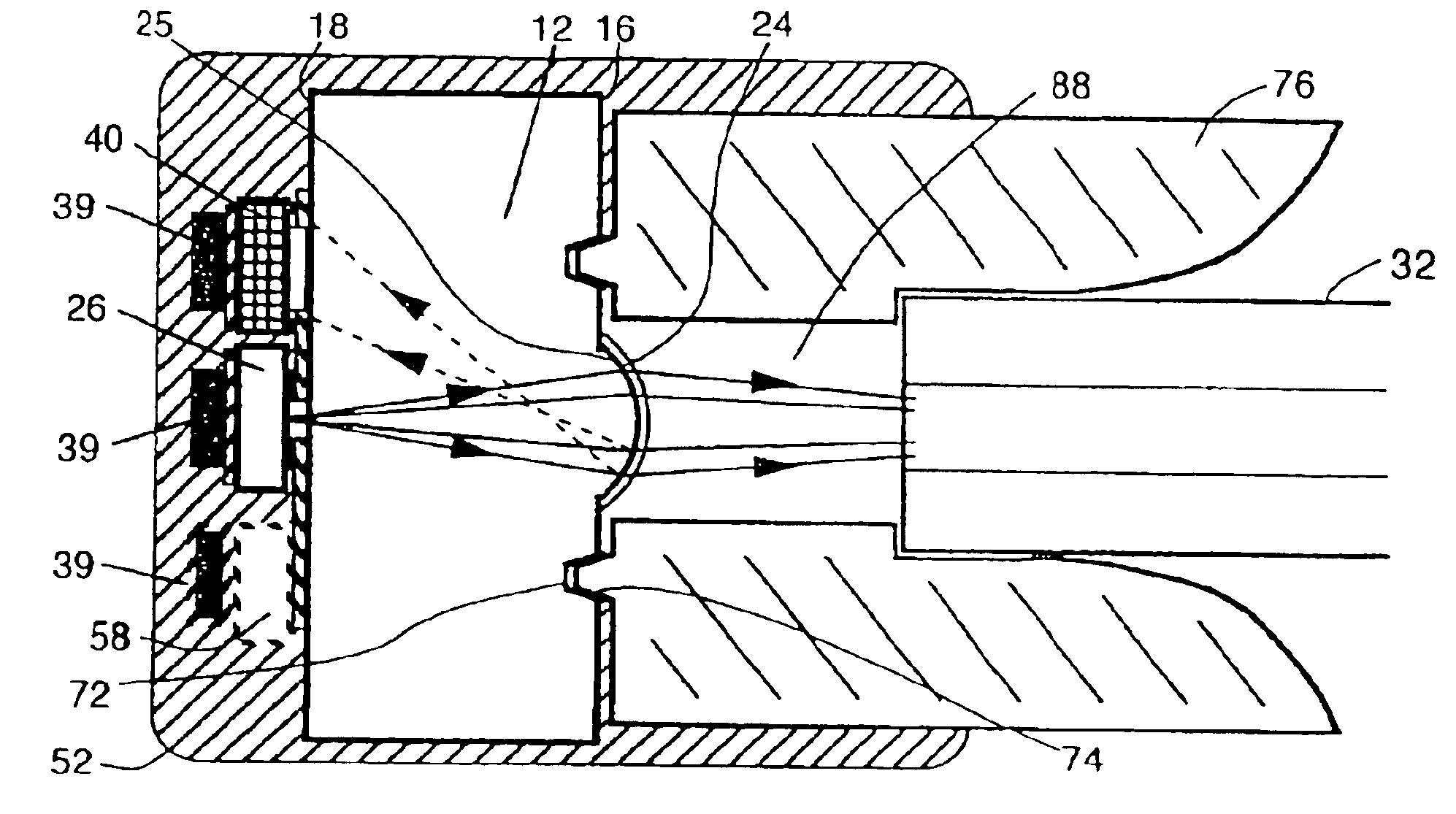
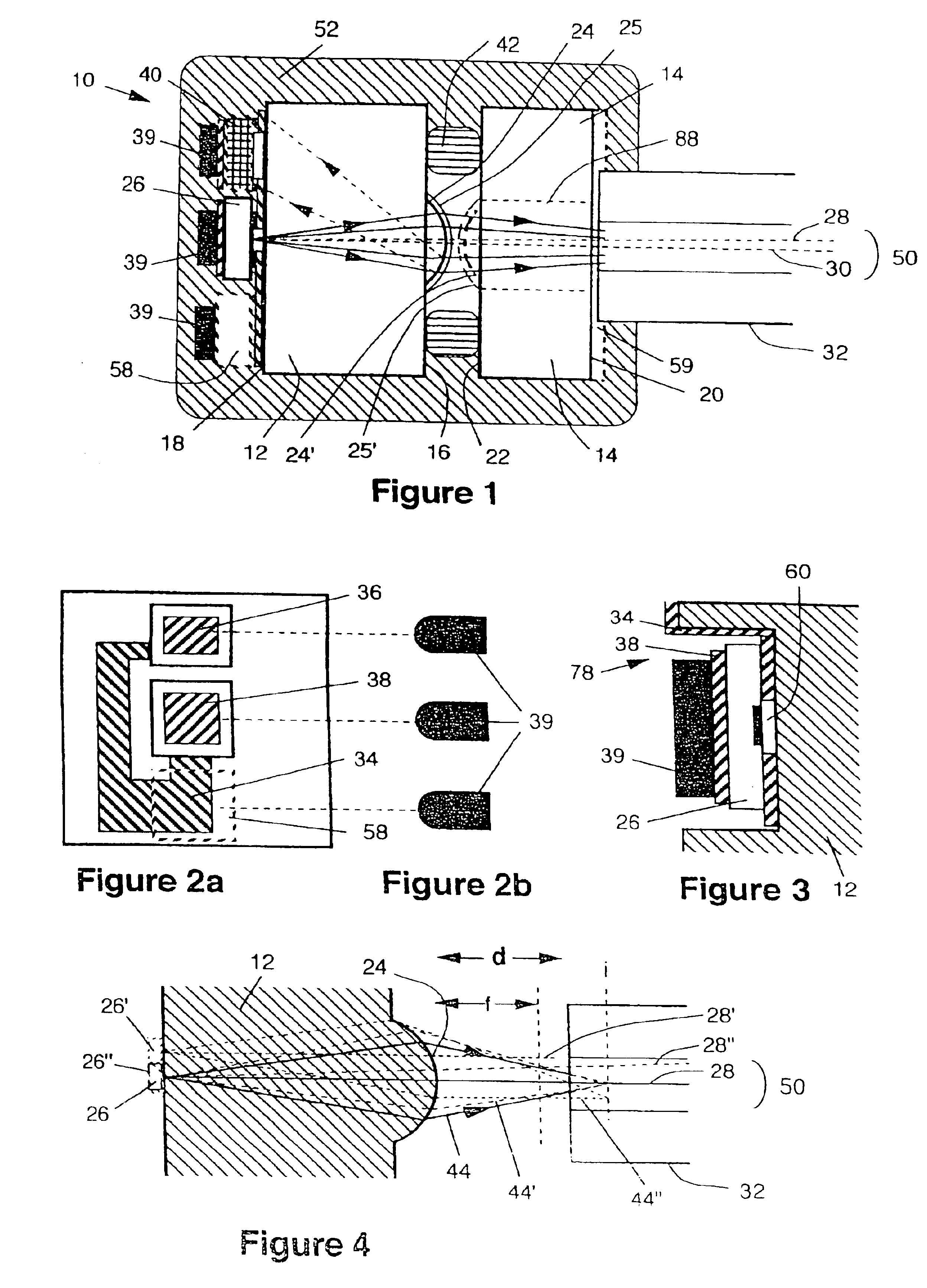
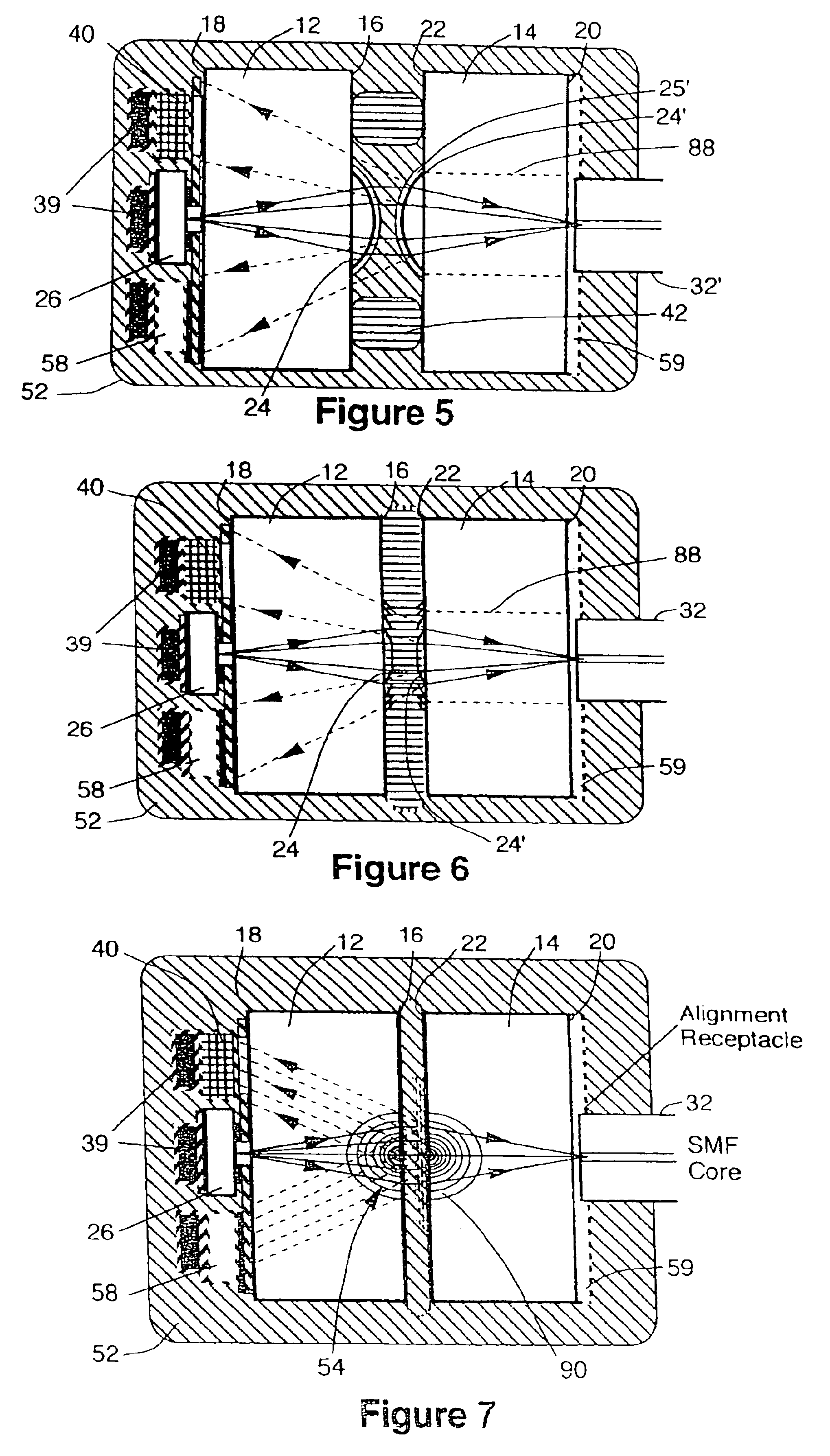
[0058]Before describing the invention, it is essential to provide definitions to terms that are used in the description of the invention. The first of these terms is an optical waveguide.
[0059]For the purposes of this patent application, an “optical waveguide” is a system of material boundaries or structures for guiding an optical wave. Such waveguides include, but are not limited to, single mode optical fibers, multi-mode optical fibers, semiconductor waveguides, dielectric waveguides, single mode polymer waveguides, and multimode polymer waveguides and optical connectors.
[0060]A single mode optical fiber (SMF) is a fiber optic cable in which only the lowest order bound mode (which may consist of a pair of orthogonal polarized fields) may propagate at the wavelength of interest. Generally, SMF has a waveguide in core diameter of ˜8 μm for wavelengths in the 1300 to 1600 nm range. It should be appreciated that the diameter of the SMF may vary while still utilizing the teachings of t...
PUM
Abstract
A novel electro-opto-mechanical assembly is provided. The electro-opto-mechanical assembly comprising: a first wafer, the wafer having a top and bottom surface; at least one optical element disposed on one surface of the first wafer; at least one discrete opto-electronic transducer element disposed on the bottom surface of the first wafer and in optical communication with the optical element; and an optical waveguide; wherein the first wafer and the optical element form an optical relay which relays light between the discrete opto-electronic transducer and the optical waveguide and thereby forms an efficient optical coupling between the discrete opto-electronic transducer and the optical waveguide.
Description
CROSS-REFERENCE TO RELATED APPLICATIONS[0001]This application is a divisional of U.S. patent application Ser. No. 10 / 351,401 entitled “Opto-Mechanical Assembly,” filed Jan. 27, 2003, now U.S. Pat. No. 6,741,777, which is a divisional application of U.S. patent application Ser. No. 10 / 092,470 entitled “Opto-Mechanical Assembly,” filed Mar. 8, 2002, now U.S. Pat. No. 6,542,672, issued Apr. 1, 2003 which is divisional application of U.S. patent application Ser. No. 09 / 822,207 entitled “Opto-Mechanical Assembly,” filed Apr. 2, 2001, now U.S. Pat. No. 6,421,474, issued Jul. 6, 2002 which is a divisional application of U.S. patent application Ser. No. 09 / 323,204 entitled “Electro-Opto-Mechanical Assembly for Coupling a Light Source or Receiver to an Optical Waveguide,” filed Jun. 1, 1999, now U.S. Pat. No. 6,243,508 issued Jun. 5, 2001. This application makes reference to the following U.S. patent application Ser. No. 08 / 905,938 entitled “Device for Coupling a Light Source or Receiver to ...
Claims
Application Information
Patent Timeline
Application Date:The date an application was filed.
Publication Date:The date a patent or application was officially published.
First Publication Date:The earliest publication date of a patent with the same application number.
Issue Date:Publication date of the patent grant document.
PCT Entry Date:The Entry date of PCT National Phase.
Estimated Expiry Date:The statutory expiry date of a patent right according to the Patent Law, and it is the longest term of protection that the patent right can achieve without the termination of the patent right due to other reasons(Term extension factor has been taken into account ).
Invalid Date:Actual expiry date is based on effective date or publication date of legal transaction data of invalid patent.