Electrostatic discharge protection circuit of non-gated diode and fabrication method thereof

Inactive Publication Date: 2005-08-23
UNITED MICROELECTRONICS CORP
View PDF18 Cites 27 Cited by
  • Summary
  • Abstract
  • Description
  • Claims
  • Application Information

AI Technical Summary

Benefits of technology

[0011]The ESD protection circuit of a non-gated diode and the fabrication method ther

Problems solved by technology

The device failure is initiated by thermal runaway and followed by catastrophic damage during an ESD pulse.
In SOI devices, the presence of the buried oxid

Method used


Image

  • Electrostatic discharge protection circuit of non-gated diode and fabrication method thereof
  • Electrostatic discharge protection circuit of non-gated diode and fabrication method thereof
  • Electrostatic discharge protection circuit of non-gated diode and fabrication method thereof

Examples


Embodiment Construction

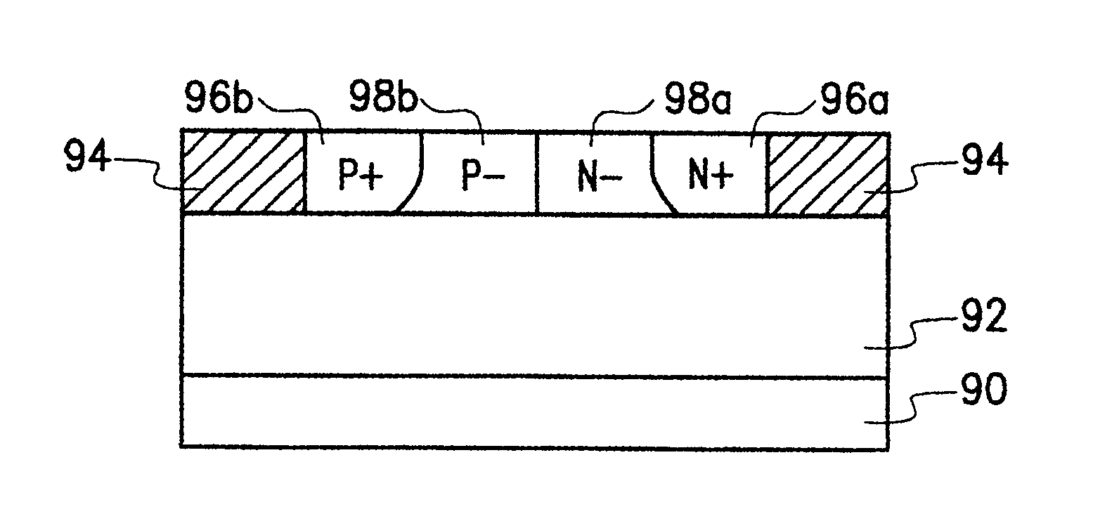
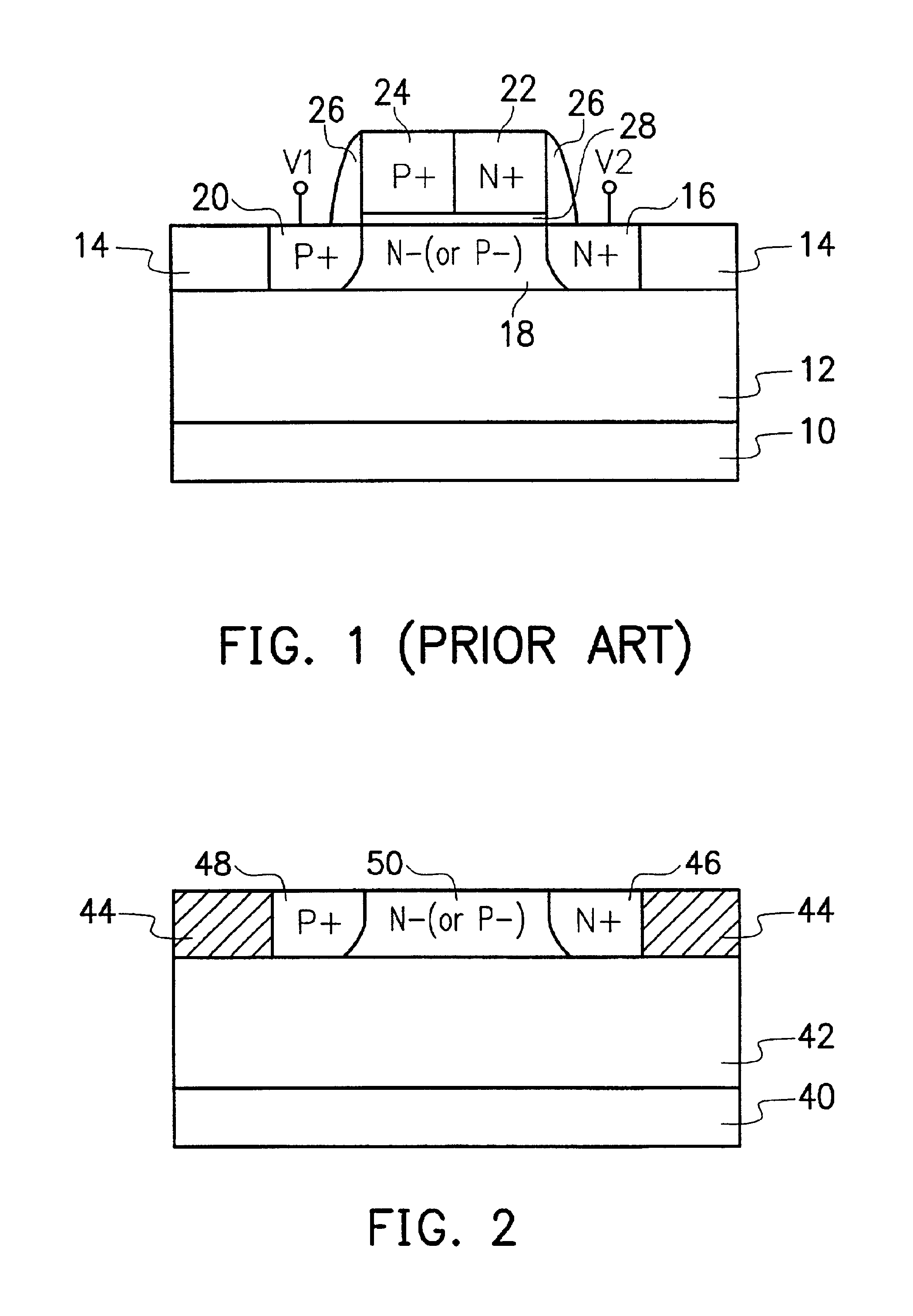
[0040]FIG. 2 is a cross-sectional view showing an embodiment of a non-gated diode with a STI-blocking structure. In FIG. 2, the SOI non-gated diode is formed on a SOI substrate that includes a substrate 40, an insulation layer 42 and a silicon layer. The substrate 40 includes either a P-type substrate or an N-type substrate. The insulation layer 42 includes a buried oxide layer. The SOI non-gated diode with the STI blocking structure is formed in the silicon layer. In the silicon layer, the SOI non-gated diode is formed between two STI blocking structures 44. That is, the doped region of the SOI non-gated diode is isolated by the two STI structures. A lightly doped well region 50 doped with P-type or N-type ions (P-well or N-well) is formed on the insulation layer 42 between the two STI structures. In addition, heavily doped P-type (P+) diffusion region 48 and heavily doped N-type (N+) diffusion region 46 are formed in the corners of the P- or N-well region 50 adjacent to the two ST...


PUM


Abstract

A non-gated diode structure of a silicon-on-insulator, having a silicon-on-insulator substrate, a pair of isolating structures, a first type doped region and a second type doped region. The silicon-on-insulation substrate has a stack of a substrate, an insulation layer and a silicon layer. The isolating structures are located in the silicon layer to define a well region. The first and second type doped regions are located in the well and are adjacent to the isolating structures. Such a non-gated diode structure can be applied to an electrostatic discharge protection circuit to increase the electrostatic discharge protection voltage or current. In addition, a fabrication method of the non-gated diode is also introduced. This non-gated diode can be also fabricated in the general bulk CMOS process, and used in the on-chip ESD protection circuits.

Description

CROSS-REFERENCE TO RELATED APPLICATION[0001]This application claims the priority benefit of Taiwan application serial no. 91101026, filed Jan. 23, 2002.BACKGROUND OF THE INVENTION[0002]1. Field of the Invention[0003]The invention relates in general to an electrostatic discharge protection circuit and a fabrication method thereof, and more particularly, to an electrostatic discharge protection circuit of a non-gated diode and a fabrication method thereof that uses the silicon-on-insulation (SOI) fabrication process.[0004]2. Description of the Related Art[0005]Silicon-on-insulator technology is a prime contender for low voltage, and high-speed applications because of its advantages over bulk-Si technology in high isolation, latch-up immunity, and smaller junction capacitance. However, electrostatic discharge (ESD) is a major concern for SOI technology.[0006]The protection level provided by an ESD protection circuit is determined by the amount of current that it can sink while clamping...

Claims


Application Information

Patent Timeline
IPC IPC(8): H01L21/70H01L27/08H01L27/02H01L27/12H01L21/84
CPCH01L21/84H01L27/0255H01L27/08H01L27/0814H01L27/1203
Inventor KER, MING-DOUHUNG, KEI-KANGTANG, TIEN-HAO
Owner UNITED MICROELECTRONICS CORP
Why Eureka
Try Eureka