
Methods and apparatus for E-beam treatment used to fabricate integrated circuit devices

a technology of electron beam treatment and integrated circuit, which is applied in the direction of coatings, special surfaces, chemical vapor deposition coatings, etc., can solve the problems of rc delay, power consumption, crosstalk, and increase the complexity of fabrication

Inactive Publication Date: 2005-08-30
APPLIED MATERIALS INC
View PDF89 Cites 59 Cited by
  • Summary
  • Abstract
  • Description
  • Claims
  • Application Information

AI Technical Summary

Benefits of technology

The present invention provides a method for making a low-k dielectric film by chemical vapor deposition and e-beam treatment. This method can improve the performance of semiconductor devices by reducing the dielectric constant of the film.

Problems solved by technology

Fabrication of integrated devices, for example, and without limitation, semiconductor integrated devices, is complicated and, due to increasingly stringent requirements on device designs due to demands for greater device speed, fabrication is becoming ever more complicated.
In the production of advanced integrated circuits that have minimum feature sizes of 0.13 μm and below, problems of RC delay, power consumption, and crosstalk become significant.
This is problematic because there is a trend (due to the types of metals used to fabricate the integrated circuits, and to reduce thermal stress) to reduce the total thermal budget of the interconnect process flow—this includes reducing peak process temperatures as well as total process time at high process temperatures.
One disadvantage of using a thermal process to achieve desired film properties is that it adds an additional process step, which includes possibly an additional process tool.
In addition, the use of spin-on-glass materials is limited in terms of thickness by their tendency to crack when made in thick layers and cured.

Method used


Image

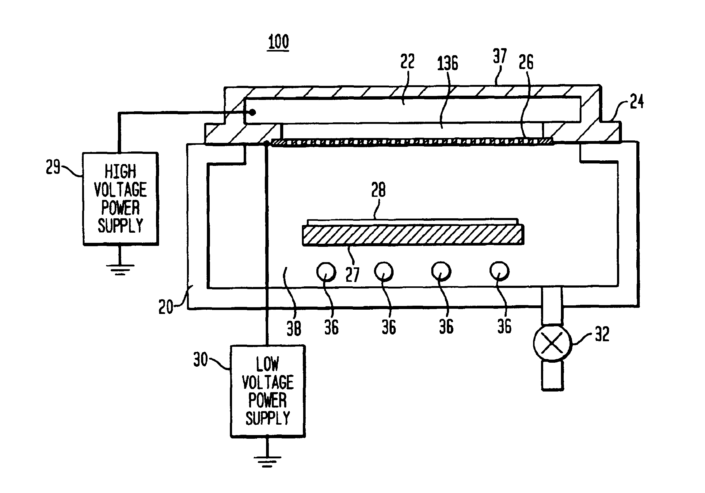
  • Methods and apparatus for E-beam treatment used to fabricate integrated circuit devices
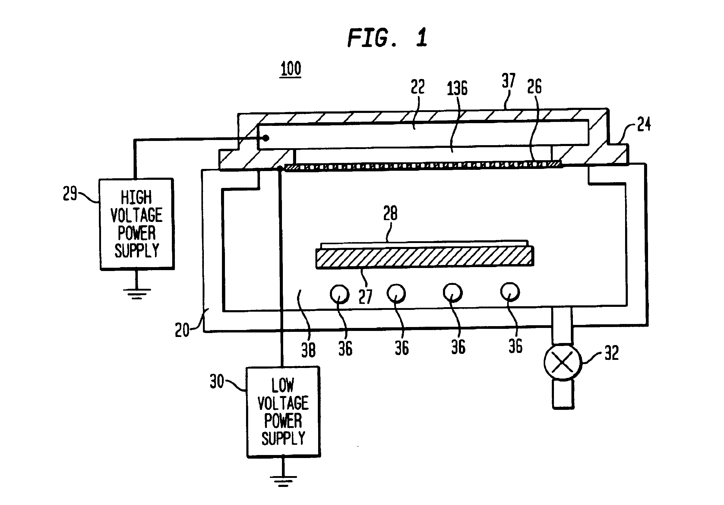
  • Methods and apparatus for E-beam treatment used to fabricate integrated circuit devices
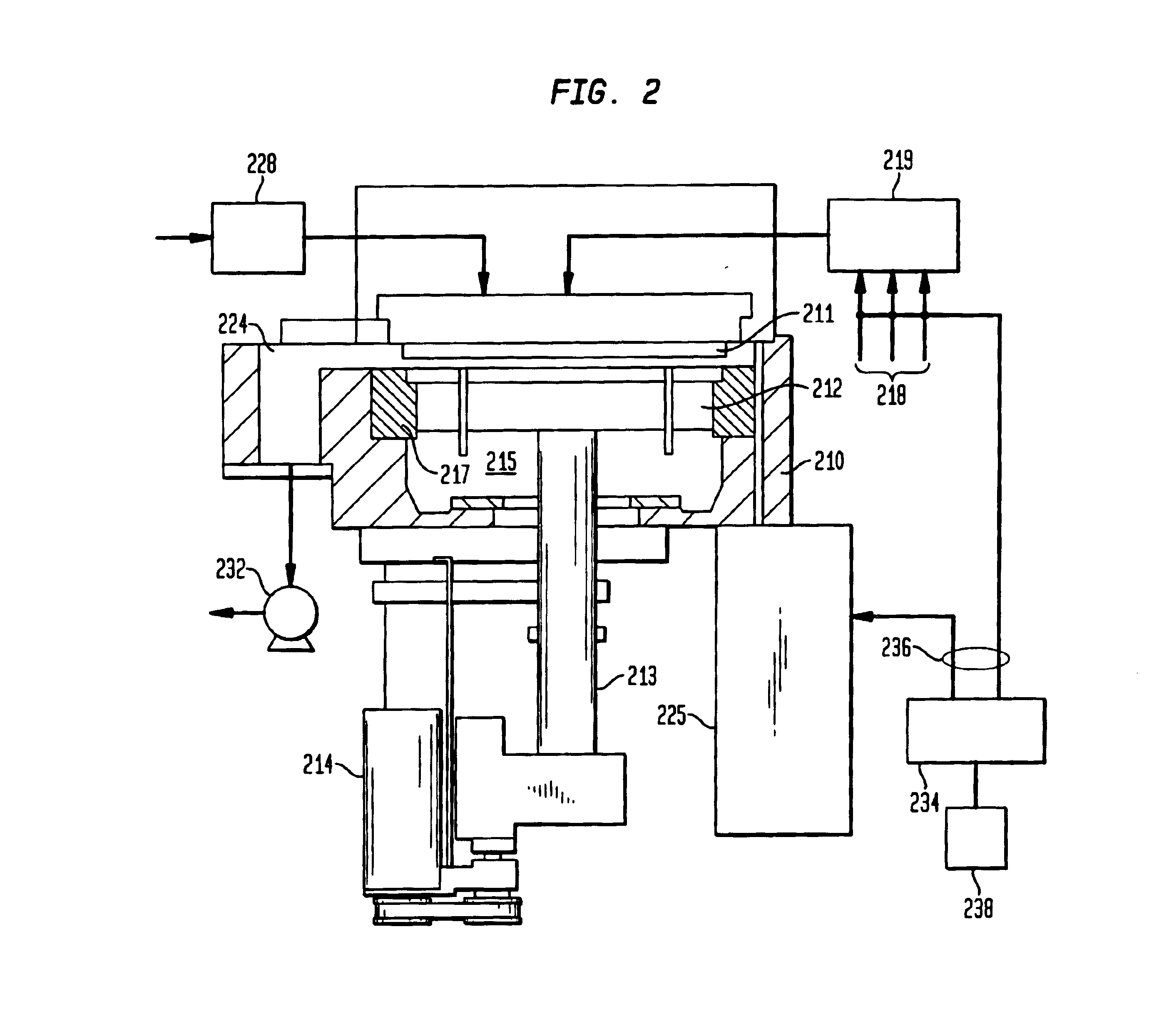
  • Methods and apparatus for E-beam treatment used to fabricate integrated circuit devices

Examples


example 3

[0087]A low dielectric constant film was deposited on a 200 mm substrate from the following reactive gases at a chamber pressure of about 6 Torr and substrate temperature of about 400° C.

[0088]Octamethylcyclotetrasiloxane (OMCTS), at about 5,000 mgm;

[0089]Trimethylsilane (TMS), at about 600 sccm;

[0090]Ethylene, at about 2,000 sccm;

[0091]Oxygen, at about 1,000 sccm; and

[0092]Helium, at about 1,000 sccm

[0093]The substrate was positioned 1,050 mils from the gas distribution showerhead. A power level of about 800 W at a frequency of 13.56 MHz was applied to the showerhead for plasma enhanced deposition of the film. The film was deposited at a rate of about 12,000 Å / min, and had a dielectric constant (k) of about 2.47 measured at 0.1 MHz.

example 4

[0094]A low dielectric constant film was deposited on a 200 mm substrate from the following reactive gases at a chamber pressure of about 6 Torr and substrate temperature of about 400° C.

[0095]Octamethylcyclotetrasiloxane (OMCTS), at about 5,000 mgm;

[0096]Trimethylsilane (TMS), at about 800 sccm;

[0097]Ethylene, at about 2,000 sccm;

[0098]Oxygen, at about 1,000 sccm; and

[0099]Helium, at about 1,000 sccm

[0100]The substrate was positioned 1,050 mils from the gas distribution showerhead. A power level of about 800 W at a frequency of 13.56 MHz was applied to the showerhead for plasma enhanced deposition of the film. The film was deposited at a rate of about 12,000 Å / min, and had a dielectric constant (k) of about 2.47 measured at 0.1 MHz.

example 5

[0101]A low dielectric constant film was deposited on a 200 mm substrate from the following reactive gases at a chamber pressure of about 6 Torr and substrate temperature of about 400° C.

[0102]Octamethylcyclotetrasiloxane (OMCTS), at about 5,000 mgm;

[0103]Trimethylsilane (TMS), at about 900 sccm;

[0104]Ethylene, at about 2,000 sccm;

[0105]Oxygen, at about 1,000 sccm; and

[0106]Helium, at about 1,000 sccm

[0107]The substrate was positioned 1,050 mils from the gas distribution showerhead. A power level of about 800 W at a frequency of 13.56 MHz was applied to the showerhead for plasma enhanced deposition of the film. The film was deposited at a rate of about 12,000 Å / min, and had a dielectric constant (k) of about 2.48 measured at 0.1 MHz.


PUM

PropertyMeasurementUnit
feature sizesaaaaaaaaaa
boiling pointaaaaaaaaaa
pressureaaaaaaaaaa

Abstract

One embodiment of the present invention is a method for fabricating a low-k dielectric film that includes steps of: (a) chemical vapor depositing a lower-k dielectric film; and (b) e-beam treating the lower-k dielectric film.

Description

[0001]This application claims the benefit of U.S. Provisional Application No. 60 / 378,799, filed on May 8, 2002 which application is incorporated herein by reference.TECHNICAL FIELD OF THE INVENTION[0002]One or more embodiments of the present invention pertain to apparatus for electron beam treatments used to fabricate integrated circuit devices.BACKGROUND OF THE INVENTION[0003]Fabrication of integrated devices, for example, and without limitation, semiconductor integrated devices, is complicated and, due to increasingly stringent requirements on device designs due to demands for greater device speed, fabrication is becoming ever more complicated. For example, integrated circuit geometries have decreased in size substantially since such devices were first introduced several decades ago. Since then, integrated circuits have generally followed a two year / half-size rule (often called Moore's Law), which means that the number of devices on a chip doubles every two years. Today's fabricat...

Claims


Application Information

Patent Timeline
Patent Type & Authority Patents(United States)
IPC IPC(8): C23C16/56C23C16/26C23C16/40H01L21/02H01L21/312B05D3/06B05D7/24H01L21/3105
CPCB05D1/60B05D3/068C08G77/50C23C16/26C23C16/401C23C16/56H01L21/0206H01L21/02063H01L21/02126H01L21/02129H01L21/02167H01L21/02211H01L21/02216H01L21/02271H01L21/02274H01L21/02282H01L21/02351H01L21/0276H01L21/0277H01L21/0337H01L21/3105H01L21/3121H01L21/3122H01L21/3146H01L21/3148H01L21/316H01L21/31625H01L21/31633H01L21/76814H01L21/76825H01L21/76829B05D3/141B05D5/08B05D5/12H01L21/31058H01L21/3125H01L21/76807H01L21/02203
Inventor MOGHADAM, FARHADZHAO, JUNWEIDMAN, TIMOTHYROBERTS, RICK J.XIA, LI-QUNDEMOS, ALEXANDROS T.
Owner APPLIED MATERIALS INC
Learn More