Non-volatile memory cells utilizing substrate trenches

a substrate trench and memory cell technology, applied in the direction of electrical equipment, semiconductor devices, instruments, etc., can solve the problems of limiting the size of a given circuit layout, and the difficulty of performing both of these functions, so as to reduce improve performance, and reduce the effect of the size of individual memory cells

Inactive Publication Date: 2005-08-30
SANDISK TECH LLC
View PDF51 Cites 107 Cited by
  • Summary
  • Abstract
  • Description
  • Claims
  • Application Information

AI Technical Summary

Benefits of technology

[0010]The present invention is directed to the use of substrate trenches in arrays of these and other types of non-volatile memory cells in order to reduce their size and/or improve their performance. In general, vertical surfaces of the trenches are used as part of the cells. More specifically, the select transistor gates are caused to protrude into substrate trenches in a manner forming at least part of the select transistor channel length along one or both of the trench sidewalls. According to a first aspect of the present invention, a source or drain diffusion is also included in the trench, having a primary advantage of reducing the size of the individual memory cells in at least one dimension. According to a second aspect of the present inventi

Problems solved by technology

It is often difficult to perform both of these functions in an optimum manner with a single voltage.
But since there are limits of how far a given circuit lay

Method used


Image

  • Non-volatile memory cells utilizing substrate trenches
  • Non-volatile memory cells utilizing substrate trenches
  • Non-volatile memory cells utilizing substrate trenches

Examples


first specific embodiment

of the Memory Cells and Array

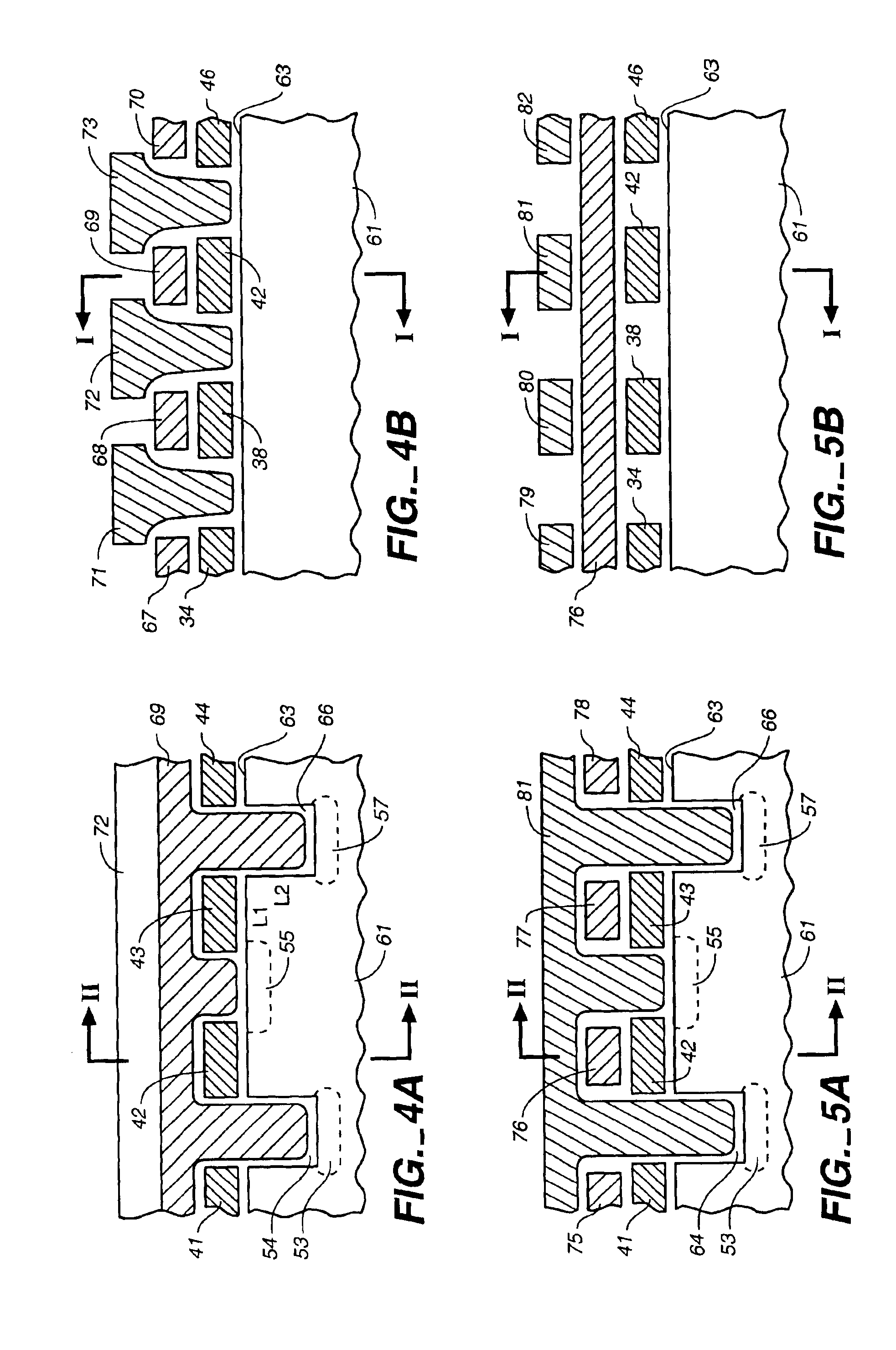
[0038]In the embodiment shown by the orthogonal cross-sectional views of FIGS. 4A and 4B, alternate diffusions are positioned across the substrate in the x-direction in the bottom of trenches in the substrate, and the remaining diffusions are formed on the substrate surface. The trenches are elongated in the y-direction and spaced apart in the x-direction. The diffusions 53 and 57, for example, are in the bottom of respective trenches 64 and 66 in the substrate 61, while the diffusion 55 is formed in the substrate surface 63. Word lines 67-70 are elongated with their lengths extending in the x-direction across the substrate over a row of floating gates, while being spaced apart in the y-direction. The word lines include select gates extending down into the trenches, as shown in FIG. 4A for the word line 69 with select gates in the trenches 64 and 66. A thin dielectric between the walls of a trench and the select gate therein provides capacitive coupling ...

second specific embodiment

of the Memory Cells and Array

[0042]The orthogonal cross-sectional views of FIGS. 5A and 5B show a second embodiment that has the same structure of floating gates, trenches and diffusions as the first embodiment but the gates formed from the second and third polysilicon layers are different. The second polysilicon layer is formed into steering gates 75-78 that are elongated in the y-direction and spaced apart across the substrate 61 in the x-direction. Each steering gate extends across a column of floating gates with which it is capacitively coupled, so that a portion of the voltage on a steering gate is coupled with the floating gates under it.

[0043]Word lines 79-82 are formed from the third polysilicon layer. As can be seen from FIG. 5A, select transistor gates extend downward from the word line 81 into the trenches 64 and 66. As with the first embodiment, the select gates are capacitively coupled with both sides of the trenches that are opposite to each other in the x-direction. T...

third specific embodiment

of the Memory Cells and Array

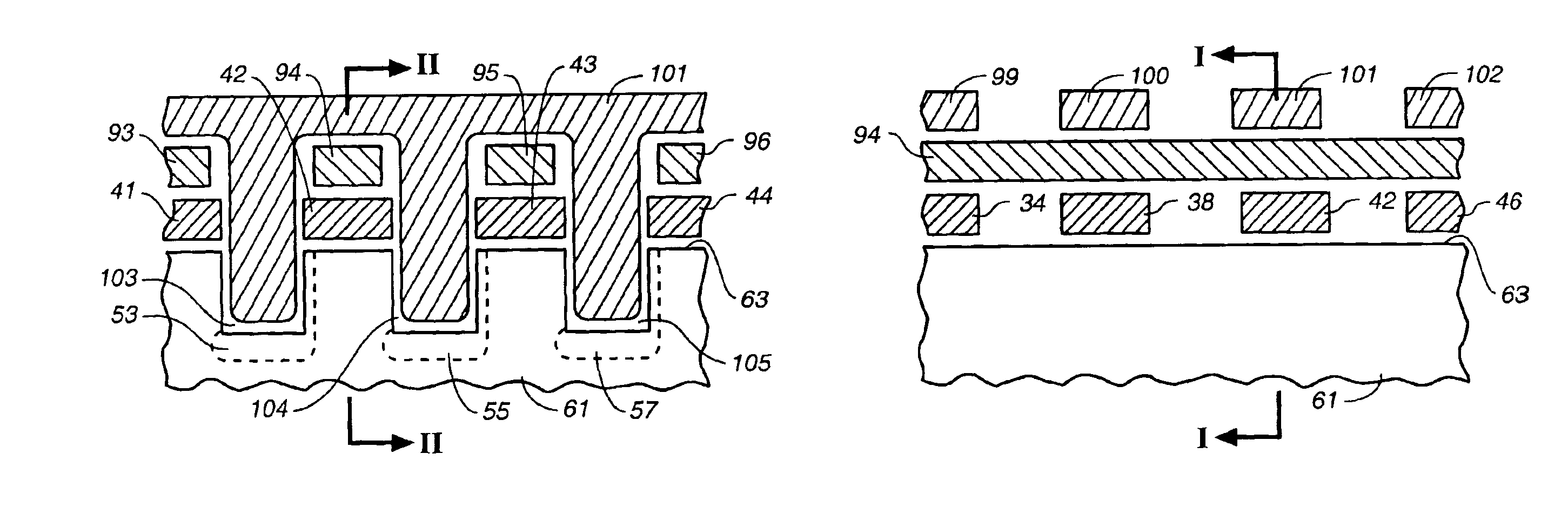
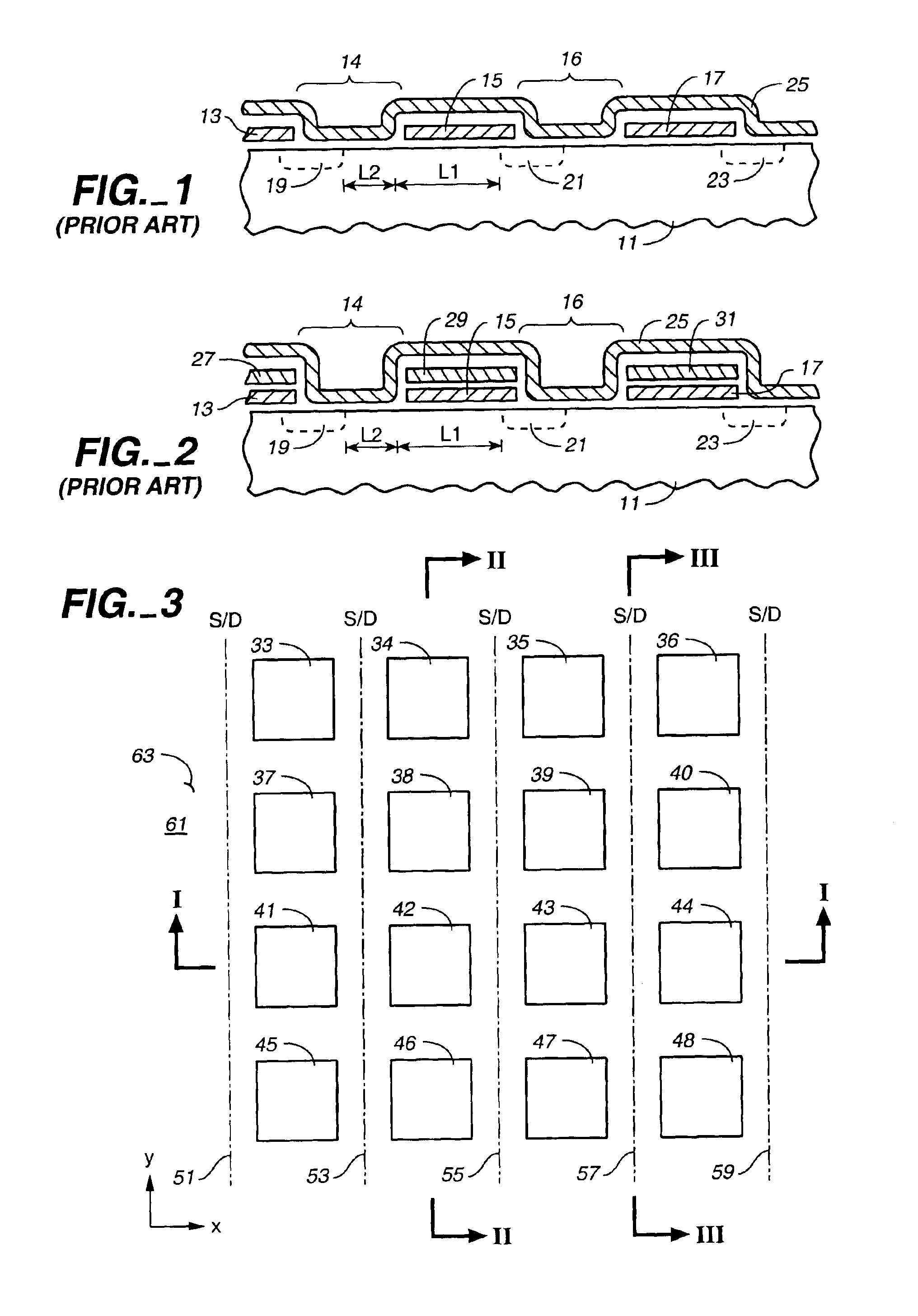
[0045]A cell array using a different trench structure than in the first and second embodiments is illustrated by the orthogonal sectional views of FIGS. 6A and 6B. In this third embodiment, trenches are provided between each column of floating gates. Trenches 103, 104 and 105 of FIG. 6A have widths that extend completely between, or almost completely between, adjacent columns of floating gates that include respective floating gates 41-44. Source and drain diffusions 53, 55 and 57 of this embodiment are formed in the bottom and up one side of respective trenches 103, 104 and 105, the sides all facing in the same direction. The select gate channel L2 of a cell is on a wall of each trench that is opposite to the wall containing the diffusion. The floating gates 41-44 remain on the substrate surface 63 and extend between trenches on either side of them in the x-direction. The sidewall portion of the diffusions extend up to the substrate surface 63 and are in...


PUM


Abstract

Several embodiments of flash EEPROM split-channel cell arrays are described that position the channels of cell select transistors along sidewalls of trenches in the substrate, thereby reducing the cell area. Select transistor gates are formed as part of the word lines and extend downward into the trenches with capacitive coupling between the trench sidewall channel portion and the select gate. In one embodiment, trenches are formed between every other floating gate along a row, the two trench sidewalls providing the select transistor channels for adjacent cells, and a common source/drain diffusion is positioned at the bottom of the trench. A third gate provides either erase or steering capabilities. In another embodiment, trenches are formed between every floating gate along a row, a source/drain diffusion extending along the bottom of the trench and upwards along one side with the opposite side of the trench being the select transistor channel for a cell. In another embodiment, select transistor gates of dual floating gate memory cells are extended into trenches or recesses in the substrate in order to lengthen the select transistor channel as the surface dimensions of the cell are being decreased. Techniques for manufacturing such flash EEPROM split-channel cell arrays are also included.

Description

CROSS-REFERENCE TO RELATED APPLICATION[0001]This is a continuation-in-part of application Ser. No. 09 / 860,704, filed May 18, 2001.FIELD OF THE INVENTION[0002]This invention relates to non-volatile flash EEPROM (Electrically Erasable and Programmable Read Only Memory) cell arrays, primarily to the structure of memory cells and to processes of manufacturing memory cell arrays.BACKGROUND[0003]There are many commercially successful non-volatile memory products being used today, particularly in the form of small cards, which use a flash EEPROM array of cells having a “split-channel” between source and drain diffusions. The floating gate of the cell is positioned over one portion of the channel and the word line (also referred to as a control gate) is positioned over the other channel portion as well as the floating gate. This effectively forms a cell with two transistors in series, one (the memory transistor) with a combination of the amount of charge on the floating gate and the voltage...

Claims


Application Information

Patent Timeline
IPC IPC(8): H01L21/70H01L27/115H01L21/8247H01L27/10H01L29/788H01L29/792
CPCH01L27/115H01L27/11521H01L27/11553G11C16/0416H10B41/23H10B69/00H10B41/30
Inventor HARARI, ELIYAHOUYUAN, JACK H.SAMACHISA, GEORGECHIEN, HENRY
Owner SANDISK TECH LLC
Why Eureka
Try Eureka