Integrated NAND and nor-type flash memory device and method of using the same

Active Publication Date: 2005-08-30
AVAGO TECH INT SALES PTE LTD
View PDF7 Cites 58 Cited by
  • Summary
  • Abstract
  • Description
  • Claims
  • Application Information

AI Technical Summary

Benefits of technology

[0018]The semiconductor memory device having both the NOR array, NAND array, and supporting interface controllers is preferably a flash semiconductor device. Moreover, the flash semiconductor memory device preferably includes a single transistor for each memory cell, regardless of whether the cell is within the NOR array or the NAND array. The single transistor may include a single floating gate dielectrically spaced between the substrate and a corresponding control gate. The floating gate within the NOR array can be programmed by hot electron injection, whereas the floating gate in the NAND array can be programmed using a tunneling mechanism. In this fashion, the NAND array can maintain its relatively fast program and erase times, while als

Problems solved by technology

Unfortunately, however, an EPROM must be packaged in a relatively expensive ceramic package with a UV-transparent window.
The amount of time needed to erase a programme

Method used


Image

  • Integrated NAND and nor-type flash memory device and method of using the same
  • Integrated NAND and nor-type flash memory device and method of using the same
  • Integrated NAND and nor-type flash memory device and method of using the same

Examples


Embodiment Construction

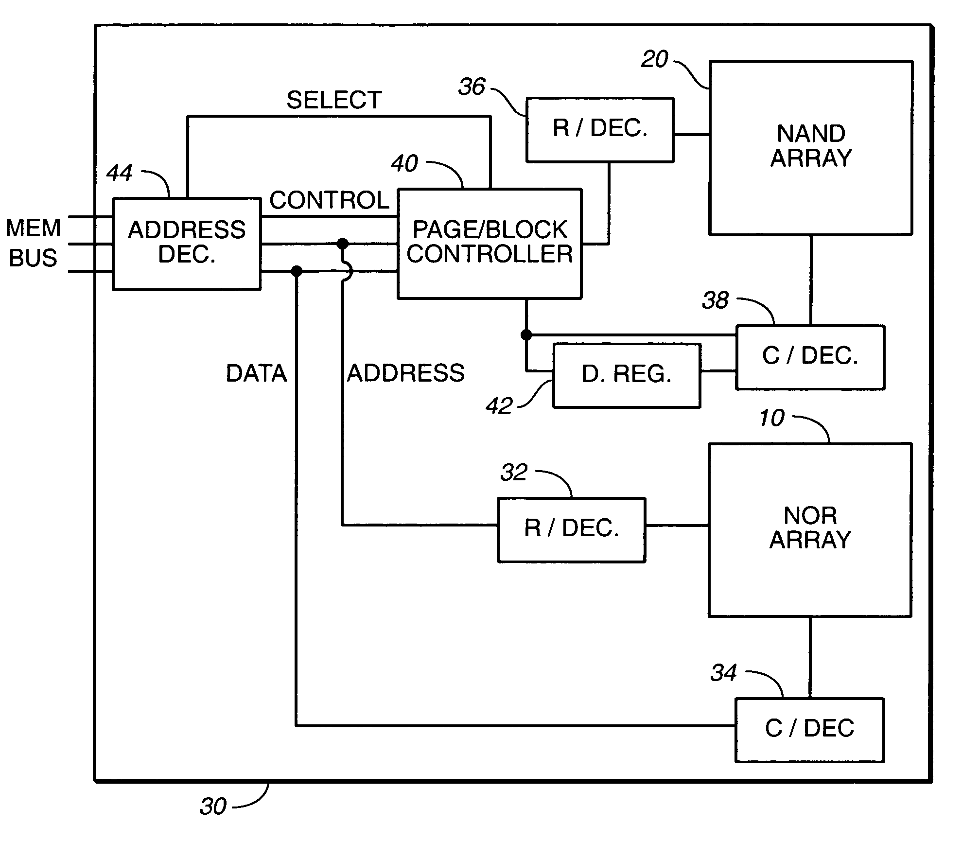
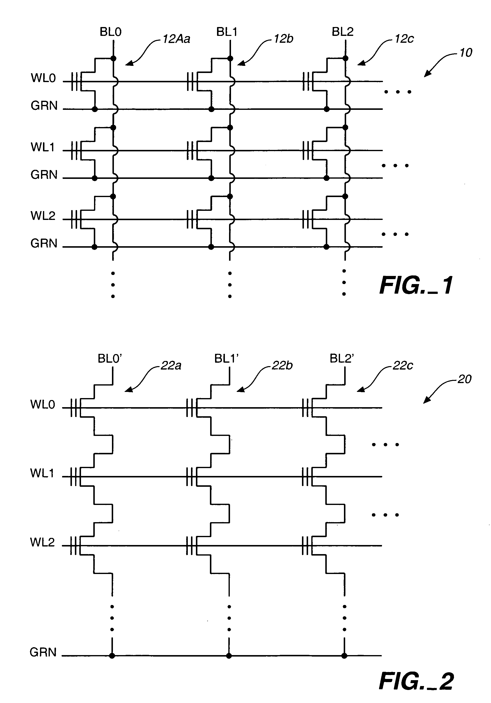
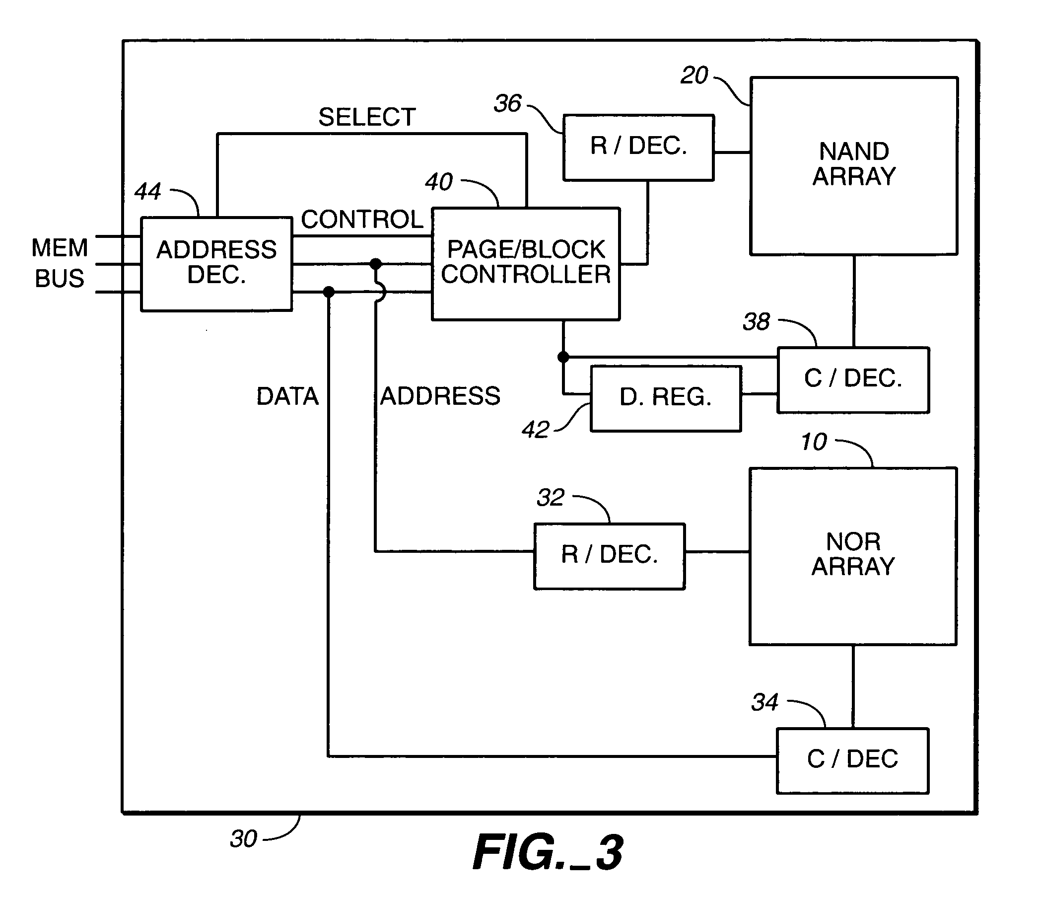
[0029]Turning now to the drawings, FIG. 1 illustrates a flash NOR array 10 within an EEPROM semiconductor memory device. More specifically, array 10, for sake of brevity and clarity in the drawing, is illustrative of only three bit lines (BL0–2) and three word lines (WL0–2) of an array having significantly more than three bit lines and word lines. The portion shown includes an array of nine flash EEPROM cells. It is certainly understood that the array can include more than three bit lines, three word lines and nine flash EEPROM cells, depending on the desired memory storage capacity. Each cell constitutes a single transistor 12. Transistor 12 can be formed as a double polysilicon gate structure. The upper polysilicon gate is referred to as the control gate, and the lower polysilicon gate is referred to as the floating gate. The gate oxide can be approximately several nanometers thick and the inter-poly dielectric can be made of nitride / oxide composite film, for example. The floating...


PUM


Abstract

A semiconductor memory device is provided as well as a method for operating the semiconductor memory device. The memory device includes a NOR array of memory cells and a NAND array of memory cells configured on the same monolithic semiconductor substrate. Each cell of the NOR array involves a single transistor, similar to each cell of the NAND array. The memory device is, therefore, an integrated circuit that includes not only the NOR and NAND arrays, but also the row and column decoders corresponding to each array. Furthermore, the integrated circuit includes the interface circuitry needed to transfer information as pages into and from the NAND array. The corresponding interface or controller is implemented on the same monolithic substrate as both the NAND array and the NOR array. Addresses targeted for the NOR array are sent as fully memory-mapped data into the NOR array, whereas addresses targeted for the NAND array are sent through the controller integrated within the semiconductor memory device. The single transistor cell of both the NAND array and NOR array preferably involves a flash EEPROM-type transistor that implements a floating gate dielectrically spaced between a control gate and the semiconductor substrate.

Description

BACKGROUND OF THE INVENTION[0001]1. Field of Invention[0002]This invention relates to semiconductor memory and, more particularly, to a NOR array and a NAND array of electrically programmable memory cells that are flash erasable, wherein both the NOR and NAND arrays are integrated upon a common substrate that can be made of predominantly single crystalline silicon.[0003]2. Description of Related Art[0004]The following descriptions and examples are not admitted to be prior art by virtue of their inclusion within this section.[0005]There are numerous types of memories available in the marketplace. For example, large volumes of data can be stored in magnetic memory, such as a hard disk drive. Lesser quantities of data can be stored in memory arranged upon an integrated circuit, oftentimes referred to as “semiconductor memory.” Semiconductor memory is typically arranged closer to the core logic unit or execution unit than the hard disk drive and can be accessed much faster than the disk...

Claims


Application Information

Patent Timeline
IPC IPC(8): G11C16/04G11C16/08
CPCG11C16/08
Inventor DESAI, GEETAKUROODI, VIJENDRALENOIR, REMI
Owner AVAGO TECH INT SALES PTE LTD
Why Eureka
Try Eureka