Quantum device
a technology of quantum devices and materials, applied in the manufacture of discharge tube main electrodes, electric discharge tubes/lamps, electric discharge systems, etc., can solve the problem of difficult to prevent the formation of natural oxide films during handling, and achieve the effect of enhancing durability
- Summary
- Abstract
- Description
- Claims
- Application Information
AI Technical Summary
Benefits of technology
Problems solved by technology
Method used
Image

Examples
first embodiment
[0036](First Embodiment)
[0037]A first embodiment of the present invention will be described below. A quantum device according to the first embodiment is an electron source adapted to emit electrons based on electric fields applied thereto, as one of electronic devices utilizing nanocrystalline silicons.
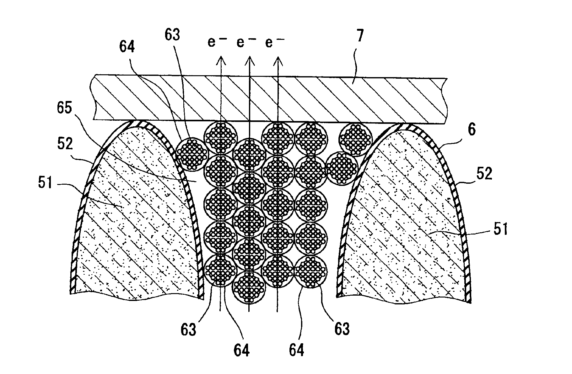
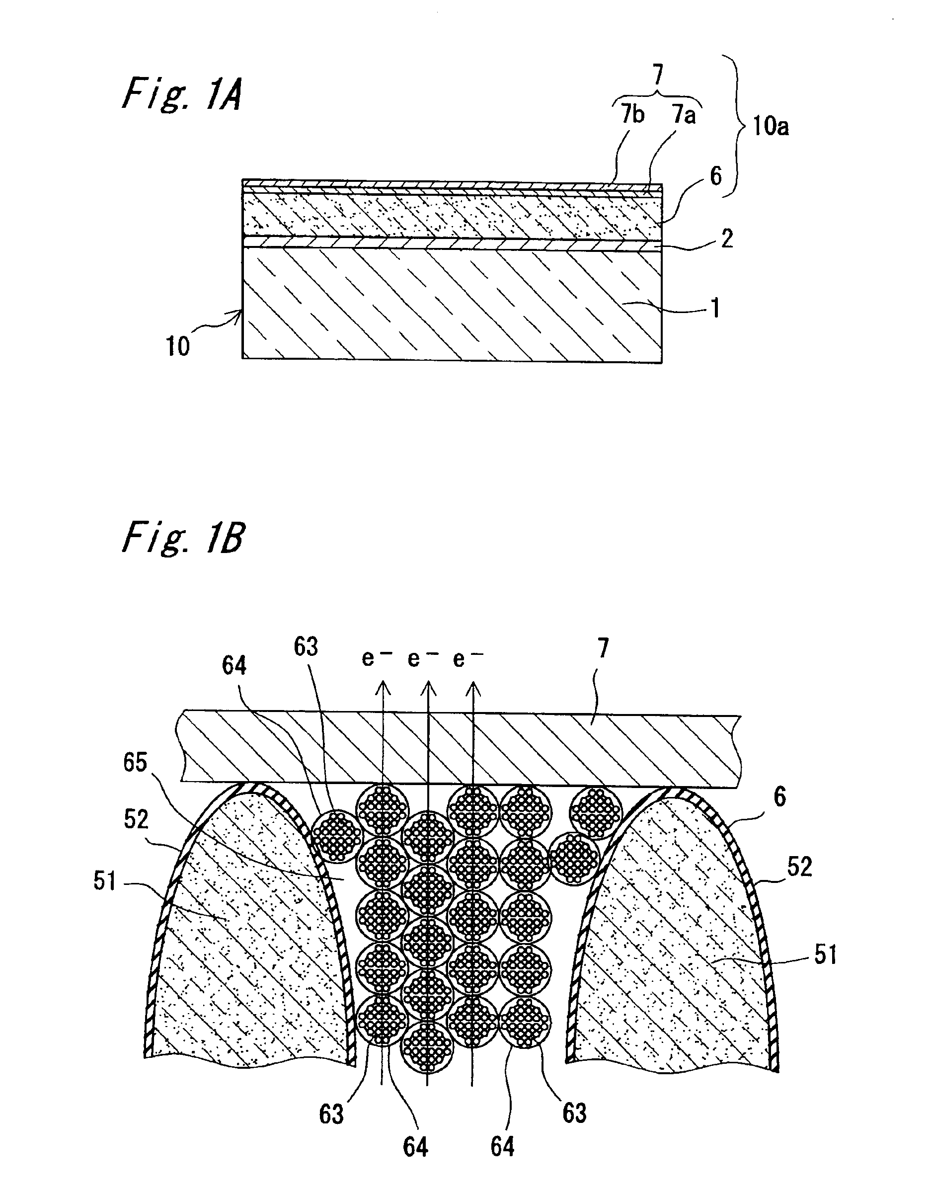
[0038]As shown in FIG. 1A, the electron source 10 according to the first embodiment includes an electron source element 10a formed on the side of one surface of an insulative substrate 1 (e.g. a glass substrate having an insulation performance or a ceramic substrate having an insulation performance). The electron source element 10a includes a lower electrode 2 formed on the side of the above surface of the insulative substrate 1, a composite nanocrystal layer 6 formed on the lower electrode 2, and a surface electrode 7 formed on the composite nanocrystal layer 6. As described in detail later, the composite nanocrystal layer 6 includes a polycrystalline silicon, and a number of nanocry...
example of first embodiment
[0061](Example of First Embodiment)
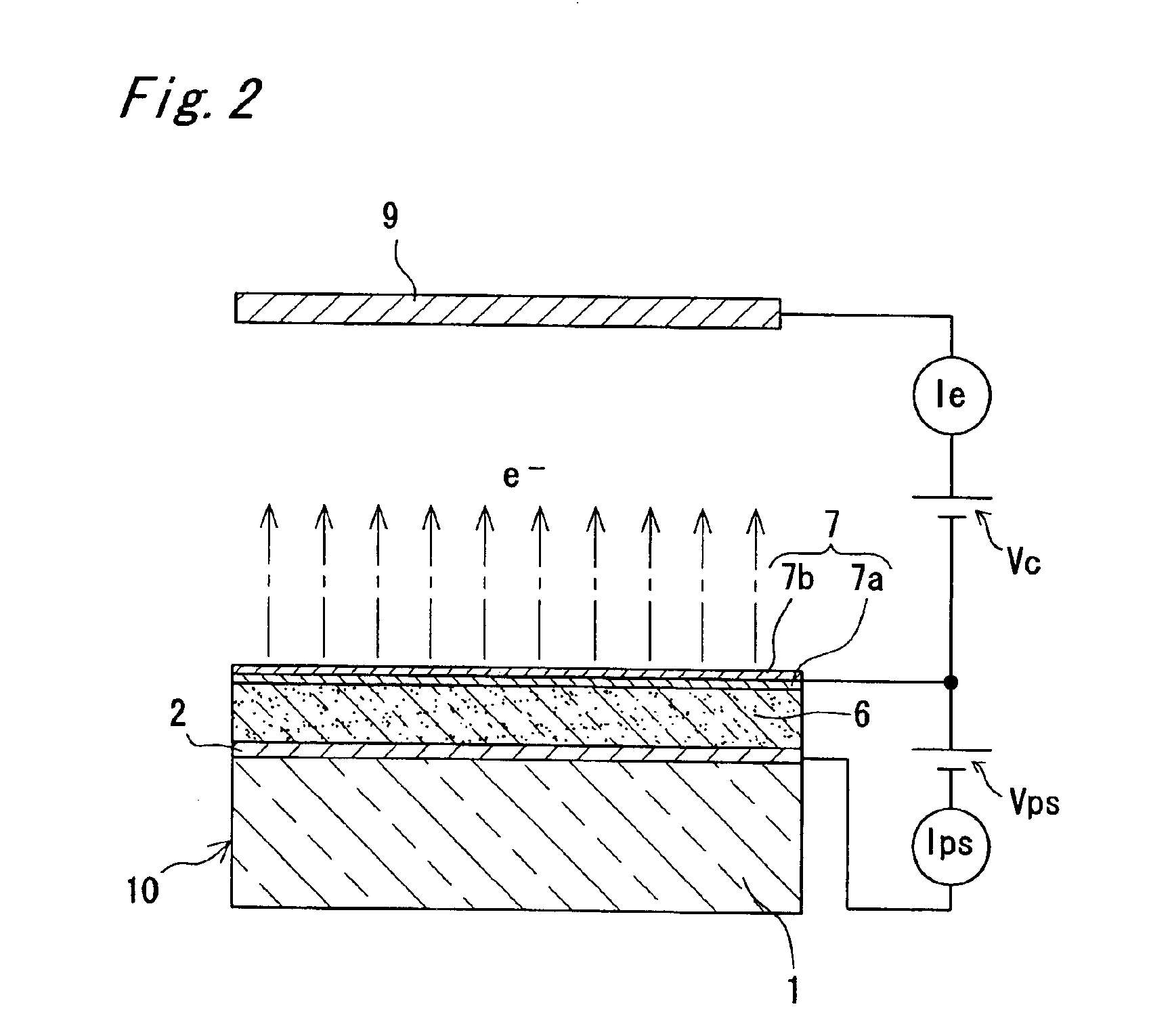
[0062]An electron source 10 as a first example was produced in accordance with the production method according to the first embodiment, and respective aging characteristic of diode current Ips and emission current Ie in the electron source 10 were measured. The measurement result is shown in FIG. 4. In the first example, an insulative substrate 1 is a glass substrate. A lower electrode 2 is a laminate film consisting of a titanium layer having a thickness of 80 nm and a tungsten layer having a thickness of 250 nm, which were formed through a sputtering method.
[0063]In the first example, a non-doped polycrystalline silicon layer 3 (see FIG. 3A) was formed through a plasma CVD method to have a thickness of 1.5 μm. The nanocrystallization process was performed by using an electrolytic solution prepared by mixing a water solution containing 55 wt % of hydrogen fluoride with ethanol at a ratio of about 1:1. In the electrolytic solution cooled down to 0°...
second embodiment
[0085](Second Embodiment)
[0086]A second embodiment of the present invention will be described below. A quantum device according to the second embodiment is a light-emitting device adapted to emit light based on electric field applied thereto, as one of electronic devices utilizing nanocrystalline silicons.
[0087]As shown in FIG. 10A, the light-emitting device 20 according to the second embodiment comprises an n-type silicon substrate 21, and an ohmic electrode 22 formed on the back surface of the n-type silicon substrate 21. A luminescent layer 26 having a number of nanocrystalline silicons 63 (see FIG. 10B) is formed on the front surface of the silicon substrate 21, and an upper electrode 27 is formed on the luminescent layer 26. In this light-emitting device 20, a lower electrode 25 is comprised of the silicon substrate 21 and the ohmic electrode 22. The luminescent layer 26 is sandwiched between the lower electrode 25 and the upper electrode 27. More specifically, the lower electr...
PUM
 Abstract
Description
Claims
Application Information