Solid-state camera including a charge coupled device

a solid-state camera and charge-coupled technology, which is applied in the direction of color television details, television systems, radio control devices, etc., can solve the problems of easy noise performance, limited equipment miniaturization effect, and easy mingling of noise in the output signal of the ccd, so as to improve noise performance and uniformity of circuit elements, the effect of reducing the number of circuit elements

Inactive Publication Date: 2005-09-06
NEC CORP
View PDF19 Cites 13 Cited by
  • Summary
  • Abstract
  • Description
  • Claims
  • Application Information

AI Technical Summary

Benefits of technology

[0027]Therefore, a primary object of the present invention is to provide a solid-state image sensor wherein is needed to field adjustment of timing pulse phases used in the signal processor or of signal balances. Another object of the invention is to provide a solid-state image sensor having noise performance more improved with a simple, miniaturized and economical configuration.
[0032]Therefore, uniformity of circuit elements can be easily attained, field adjustment of phases of timing pulses being made unnecessary, as well as realization of further miniaturization of the equipment. The noise performance is also improved, since wiring paths connecting circuit elements in the timing pulse generator and the on-chip signal processor can be shortened.
[0033]The on-chip signal processor may further comprise an A / D converter for converting output of the AGC circuit into a digital signal for enabling a user to select either of analog output or digital output.

Problems solved by technology

However, there are following problems in these prior arts.
The first problem is that only a part of peripheral circuits is configured on the same semiconductor chip of the solid-state image sensor in every of the prior arts.
The second problem is that the miniaturization effect of the equipment is limited even when a part of peripheral circuits is configured on-chip.
The third problem is that noises are susceptible to be mingled in the output signal of the CCD, even when the frequency divider is configured on the solid-state image sensor chip as described in the above Provisional Publication No. 259668 / '89.
This makes noise performance easily dependent of length or path of wirings or arrangement of equipment parts.

Method used


Image

  • Solid-state camera including a charge coupled device
  • Solid-state camera including a charge coupled device
  • Solid-state camera including a charge coupled device

Examples


Embodiment Construction

[0047]Now, embodiments of the present invention will be described in connection with the drawings.

[0048]FIG. 1 is a block diagram illustrating a configuration of an embodiment of the invention.

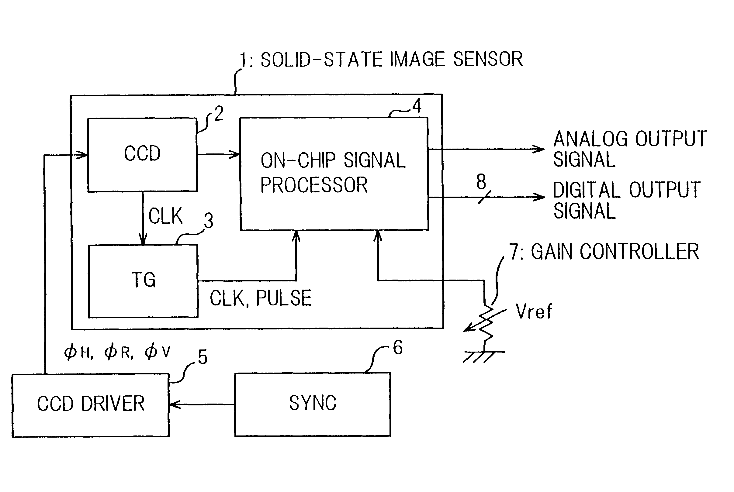
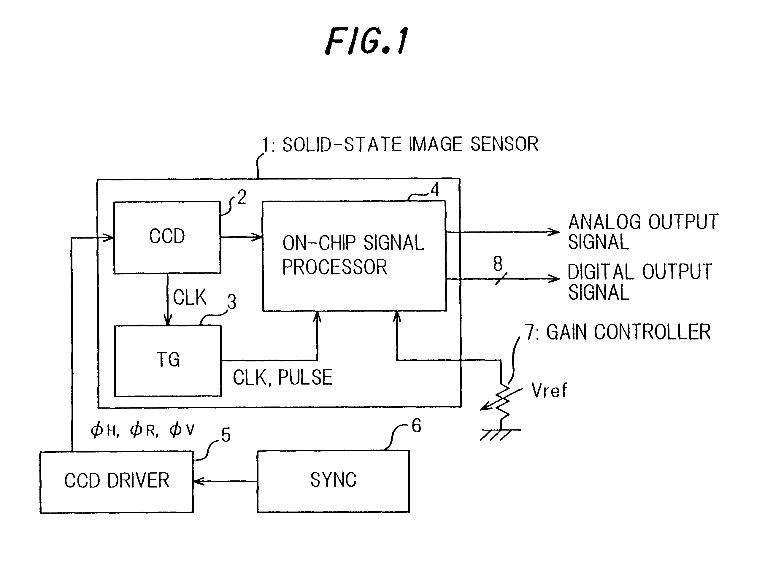
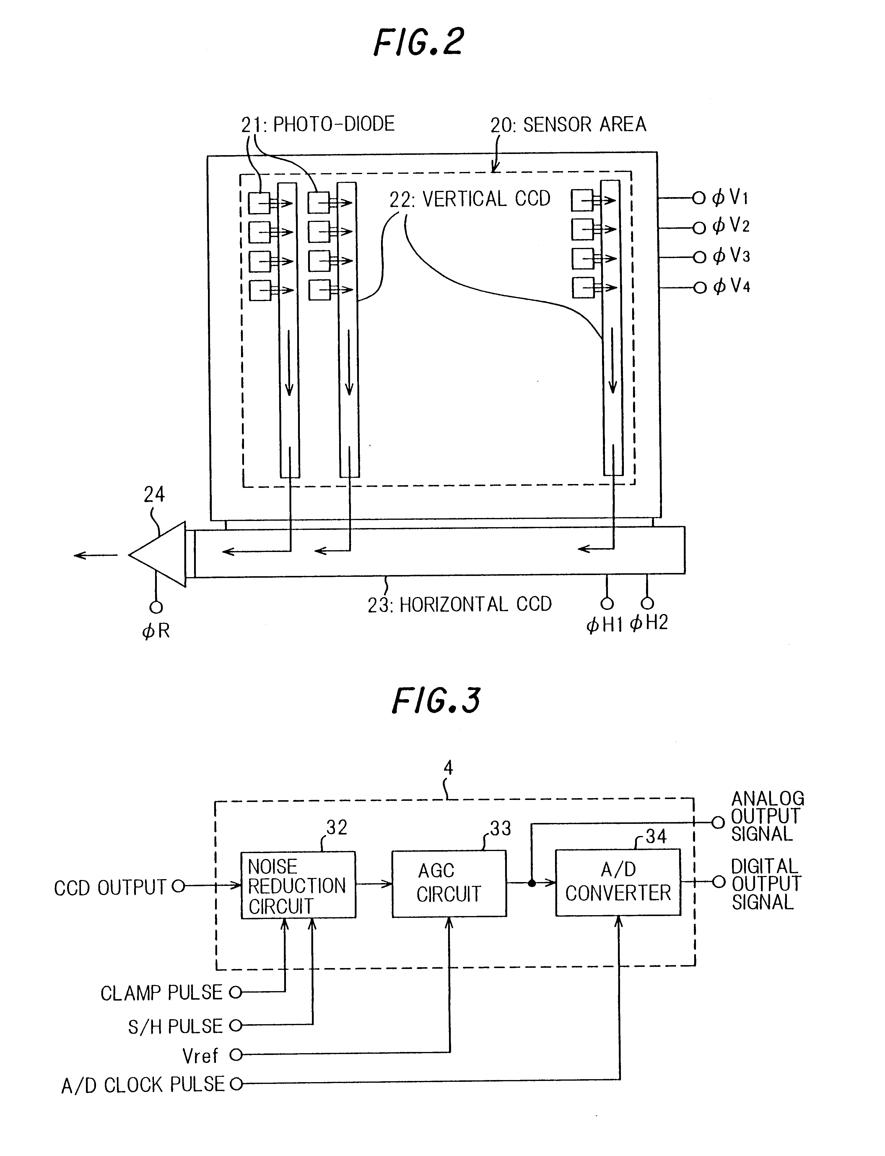
[0049]Referring to FIG. 1, a solid-state image sensor 1 according to the embodiment is configured on a semiconductor chip and comprises a CCD 2, a timing pulse generator (hereafter abbreviated as TG) 3 and an on-chip signal processor 4 including a noise reduction circuit, an auto gain control circuit (AGC) and an A / D converter.

[0050]Outside the solid-state image sensor 1, a CCD driver 5, a synchronous signal generator (hereafter abbreviated as SYNC) 6, and a gain controller 7 are provided.

[0051]CCD driving pulses (φV, φH and φR) are generated by the SYNC 6 and supplied to the CCD driver 5 to be voltage-amplified for driving the CCD 2 on the solid-state image sensor 1. Output signal of the CCD 2 is transferred to the on-chip signal processor 4, whereby processings of noise reduction, AGC and A / ...


PUM


Abstract

To provide a solid-state image sensor, wherein no field adjustment of timing pulse phases used in the signal processor or of signal balances is needed, and noise performance is more improved, with a simple, miniaturized and economical configuration, a solid-state image sensor (1) of the invention comprises: a CCD (2) configured on a semiconductor chip for generating a CCD signal according to an optical image focused on a sensor area thereof; an on-chip signal processor (4) configured on the semiconductor chip by way of the same fabrication process with the CCD including a noise reduction circuit for eliminating noises from the CCD signal, an AGC circuit for amplifying output of of the noise reduction circuit; and a timing pulse generator (3) configured on the semiconductor chip by way of the same fabrication process with the CCD (2) for generating timing pulses used the on-chip signal processor. The on-chip signal processor (4) of the solid-state image sensor (1) may further comprise an A / D converter for converting output of the AGC circuit into a digital signal.

Description

BACKGROUND OF THE INVENTION[0001]The present invention relates to a solid-state image sensor.[0002]FIG. 8 is a block diagram illustrating a conventional solid-state camera, wherein a charge coupled device (hereafter abbreviated as CCD) is applied, comprising a CCD 91, a signal processor 97, a video processor 98, a CCD driver 92 and a timing signal generator 93.[0003]FIG. 9 is a schematic diagram illustrating a configuration of the CCD 91, wherein an object image is focused on a sensor area (photoelectric transducer section) 100, and converted into electric charges corresponding to intensity of incident light by photo-diodes 101. Generated electric charges are transferred to vertical CCDs 102 through reading transfer gates. The vertical CCDs 102 are driven by vertical transfer pulses φV1 to φV4 and transfer the electric charges horizontal CCD 103 in order. The horizontal CCD 103 is driven by horizontal transfer pulses φH1 and φH2 and transfers the electric charges to an output amplif...

Claims


Application Information

Patent Timeline
Patent Type & Authority Patents(United States)
IPC IPC(8): H01L27/148H04N3/14H04N5/335H04N5/341H04N5/357H04N5/363H04N5/369H04N5/372H04N5/376H04N5/378
CPCH04N5/365H04N5/3728H04N25/67H04N25/73
Inventor KATOH, SATOSHI
Owner NEC CORP
Why Eureka
Try Eureka