Electronic device substrate assembly with multilayer impermeable barrier and method of making

a technology of electronic devices and substrates, applied in the direction of electrical apparatus casings/cabinets/drawers, lighting and heating apparatus, instruments, etc., can solve the problems of increasing device temperature, power dissipation, and therefore heat production, and achieve the effect of high effective thermal conductivity path

Inactive Publication Date: 2005-09-06
GLOBALFOUNDRIES US INC
View PDF21 Cites 45 Cited by
  • Summary
  • Abstract
  • Description
  • Claims
  • Application Information

AI Technical Summary

Benefits of technology

[0014]It is therefore an object of the present invention to provide an electronic device assembly which is capable of being placed in contact with cooling fluids such as water or other aqueous fluids, providing a high effective thermal conductivity path between electronic devices to be cooled and the cooling fluid, while preventing direct physical contact between the electronic devices to be cooled and the cooling fluid.
[0016]It is a further object of the present invention to provide a water-coolable electronic module assembly, characterized by a high effective thermal conductivity path between electronic devices to be cooled and a cooling fluid, while preventing direct contact between the electronic devices and the cooling fluid.

Problems solved by technology

This heat should be removed from the devices in order to maintain device junction temperatures within desirable limits: failure to remove the heat thus produced results in increased device temperatures, potentially leading to thermal runaway conditions.
First, power dissipation, and therefore heat production, increases as the device operating frequencies increase.
Finally, as more and more devices are packed onto a single chip, power density (Watts / cm2) increases, resulting in the need to remove more power from a given size chip or module.
These trends have combined to create applications where it is no longer desirable to remove the heat from modern devices solely by traditional air cooling methods, such as by using traditional air cooled heat sinks.
In particular, fluids such as refrigerants or other dielectric fluids exhibit relatively poor thermal conductivity and specific heat properties, when compared to fluids such as water or other aqueous fluids.
Water-based coolants, however, must be kept from physical contact with electronic devices and interconnects, since corrosion and electrical short circuit problems are likely to result from such contact.
An additional problem may arise with the use of a barrier, where the barrier material differs from any of the other materials used to construct the electronic module assembly.
This difference in expansion rates results in mechanical stresses in the structure, as the temperature of the structure varies in either direction from the temperature at which the devices were bonded (zero stress condition).

Method used


Image

  • Electronic device substrate assembly with multilayer impermeable barrier and method of making
  • Electronic device substrate assembly with multilayer impermeable barrier and method of making
  • Electronic device substrate assembly with multilayer impermeable barrier and method of making

Examples


embodiment 760

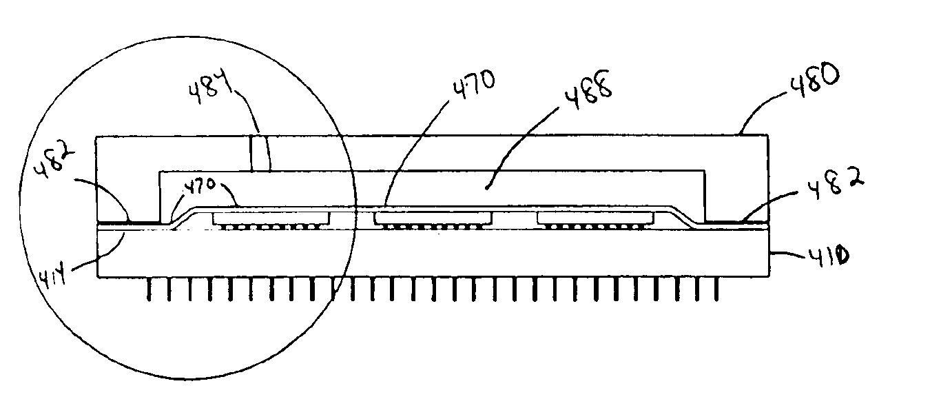
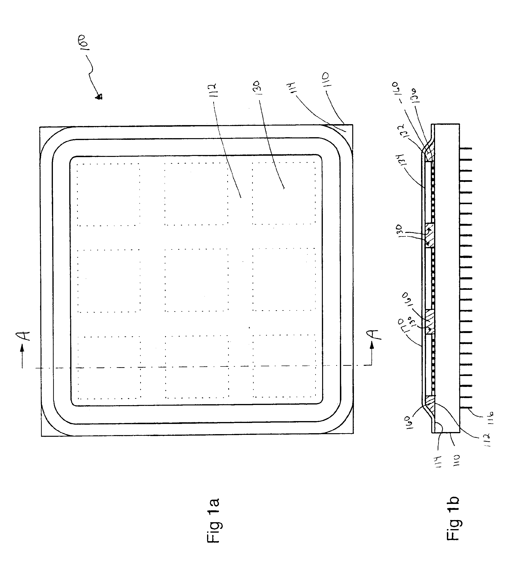
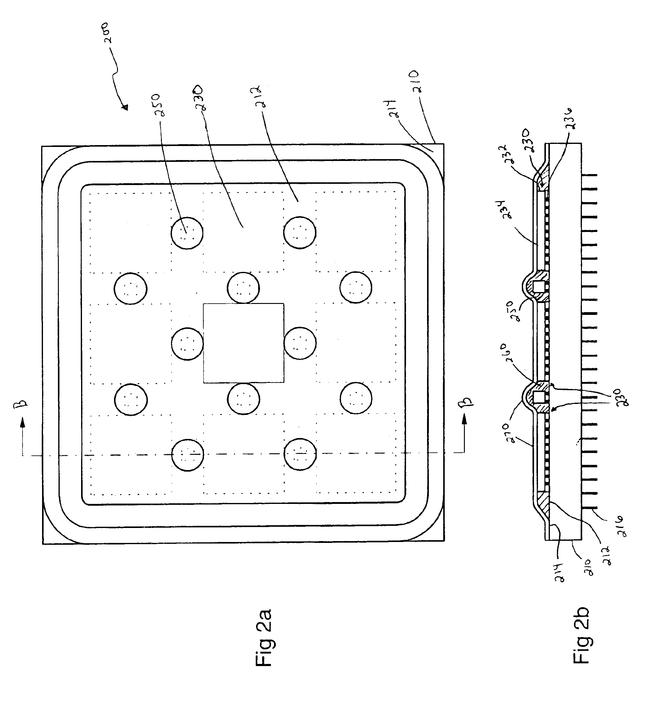
[0043]FIG. 1B further illustrates the multilayer passivation structure of the present invention. A first passivation layer 160 substantially occupies the volume adjacent to device assemblies 130, within the area bounded by substrate perimeter area 114, and extending vertically from substrate upper surface 112 to approximately the height of device assembly upper surface 134. As illustrated in FIG. 1B, first passivation layer 160 need not occupy the volume between devices 132 and substrate upper surface 112. First passivation layer 160 may, however, optionally occupy the volume between electronic device 132 and substrate upper surface 112, thereby substantially surrounding connections 136 (see first passivation layer embodiment 760, illustrated in FIG. 7C). A second passivation layer 170 is located above the first passivation layer and above the device assembly upper surfaces 134. Second passivation layer 170 is in contact with device upper surfaces 134, and thermally coupled thereto....

third embodiment

[0062]A variety of process embodiments may be used to apply the first passivation layer, and to expose the device assembly upper surfaces, in keeping with the spirit and scope of the present invention. Three exemplary embodiments are described in detail herein; a summary of these exemplary embodiments is now provided. Other process embodiments are envisioned, within the spirit and scope of the present invention, and are considered part of the invention. One exemplary embodiment involves the application of a uniform or conformal first passivation layer over a substrate subassembly, followed by selective removal of portions of the first passivation layer, thereby exposing device assembly upper surfaces. A second exemplary embodiment involves a selective application of a first passivation layer around the device assemblies and covering passive devices, while leaving device assemblies exposed. An optional uniform exposure step follows, to insure full exposure of device assembly upper su...


PUM


Abstract

An electronic module, substrate assembly, and fabrication method, the assembly providing thermal conduction between an electronic device to be cooled and an aqueous coolant, while maintaining physical separation between the coolant and electronic device. The assembly includes a substrate, one or more electronic devices to be cooled, and a multilayer, impermeable barrier. The multilayer barrier includes a first layer, providing mechanical support for a second layer. The second, thinner layer provides an impermeable barrier, and a high effective thermal conductivity path between an electronic device and a cooling fluid in contact with an upper surface of the second barrier layer. Mechanical stresses are minimized by appropriate material selection for the first layer, and a thin second layer. When incorporated into an electronic module assembly including a module cap, the substrate assembly provides physical separation between a cooling fluid introduced into the module cap, and both the substrate and electronic devices.

Description

CROSS REFERENCE TO RELATED APPLICATIONS[0001]This application contains subject matter which is related to the subject matter of the following applications, each of which is assigned to the same assignee as this application and each of which is hereby incorporated herein by reference in its entirety:[0002]“Electronic Device Substrate Assembly with Impermeable Barrier and Method of Making,” Chu et al., having, Ser. No. 10 / 047497, filed Nov. 9, 2001; and[0003]“Enhanced Air Cooling of Electronic Devices using Fluid Phase Change Heat Transfer,” Chu et al., having, Ser. No. 10 / 040680, filed Nov. 9, 2001.FIELD OF THE INVENTION[0004]The present invention relates in general to devices used for removing heat from electronic modules, and methods of constructing such devices. In particular, the present invention relates to a passivated electronic module substrate assembly, which provides a high effective thermal conductivity path between electronic devices to be cooled and a cooling fluid, whil...

Claims


Application Information

Patent Timeline
Patent Type & Authority Patents(United States)
IPC IPC(8): H01L23/31H01L23/42H01L23/34H01L23/433H01L23/473H01L23/28H01L23/00
CPCH01L23/3121H01L23/42H01L23/4334H01L23/4338H01L23/473H01L23/564H01L2224/16H01L2224/73253H01L2924/01078H01L2924/01079H01L2924/09701H01L2924/15312H01L2924/16152H01L2924/00014H01L2224/0401
Inventor CHU, RICHARD C.ELLSWORTH, JR., MICHAEL J.SIMONS, ROBERT E.SINGH, PRABJITZUCCO, PAUL A.
Owner GLOBALFOUNDRIES US INC
Why Eureka
Try Eureka