Memory system and control method for the same

a memory system and control method technology, applied in the field of memory systems, can solve the problems of timing mismatches, inability to analogize the timing relationship between the address command signal, the data signal and the clock signal, and the inability to analogize the specific configuration for transferring address command signals and data signals to and from the drams by utilizing the timing relationship, so as to reduce the clock generation the effect of reducing the clock frequency of the data signal

Inactive Publication Date: 2005-09-06
LONGITUDE SEMICON S A R L
View PDF7 Cites 19 Cited by
  • Summary
  • Abstract
  • Description
  • Claims
  • Application Information

AI Technical Summary

Benefits of technology

[0026]Preferably, the memory controller decreases the clock frequency of a data signal and also decreases a sampling frequency after retaining the phase, while the phase adjusting means of the device includes a unit for adjusting subsequent data phases according to the sampling clock after retaining the phase thereby to cause normal data transmission to take place while a sampling clock is being produced.
[0027]According to a further aspect of the present invention, there is provided a memory system including a memory controller for genera

Problems solved by technology

Hence, it is impossible to analogize the timing relationship among the address command signals, the data signals and the clock signals, and also impossible to analogize any specific configuration for transferring address command signals and data signals to and from the DRAMs by utilizing the timing relationship.
In the case of quoted example 1, the address signals, the command signals and the clock signals are all buffered on the modules, so that the signal timings at the D

Method used


Image

  • Memory system and control method for the same
  • Memory system and control method for the same
  • Memory system and control method for the same

Examples


Embodiment Construction

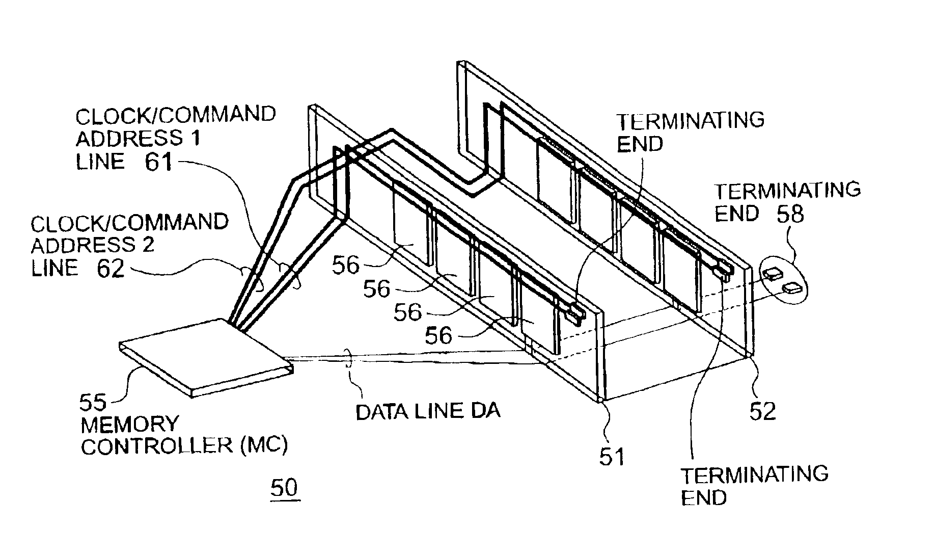
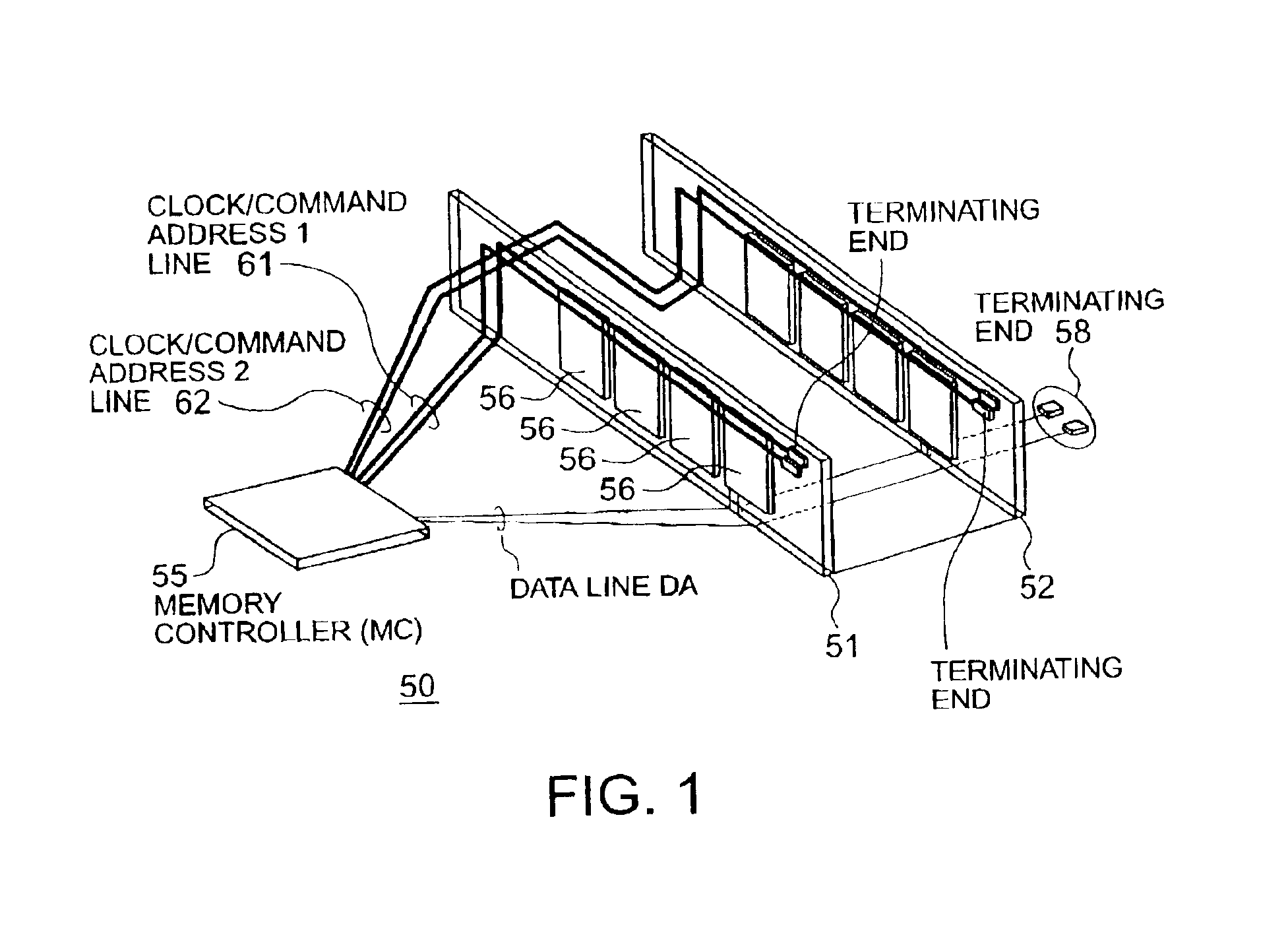
[0119]Referring to FIG. 1, the configuration of a memory system in accordance with the invention will be schematically explained. The memory system shown in the figure has a memory controller (MC) 55 mounted on a motherboard 50, and a first module 51 and a second module 52 provided in a standing manner on the motherboard 50 through a connector (not shown). In this example, the front and back surfaces of the modules 51 and 52 are provided with a plurality of memory devices (DRAMs in this case) 56 arranged in parallel, as illustrated. More specifically, the DRAMs 56 are disposed in parallel with gaps provided therebetween with respect to the direction crossing the lengthwise direction (i.e., the direction of the short sides) of the modules 51 and 52. The present invention can be also applied to a case where a plurality of memory devices is disposed on either the front or the back of the modules 51 and 52.

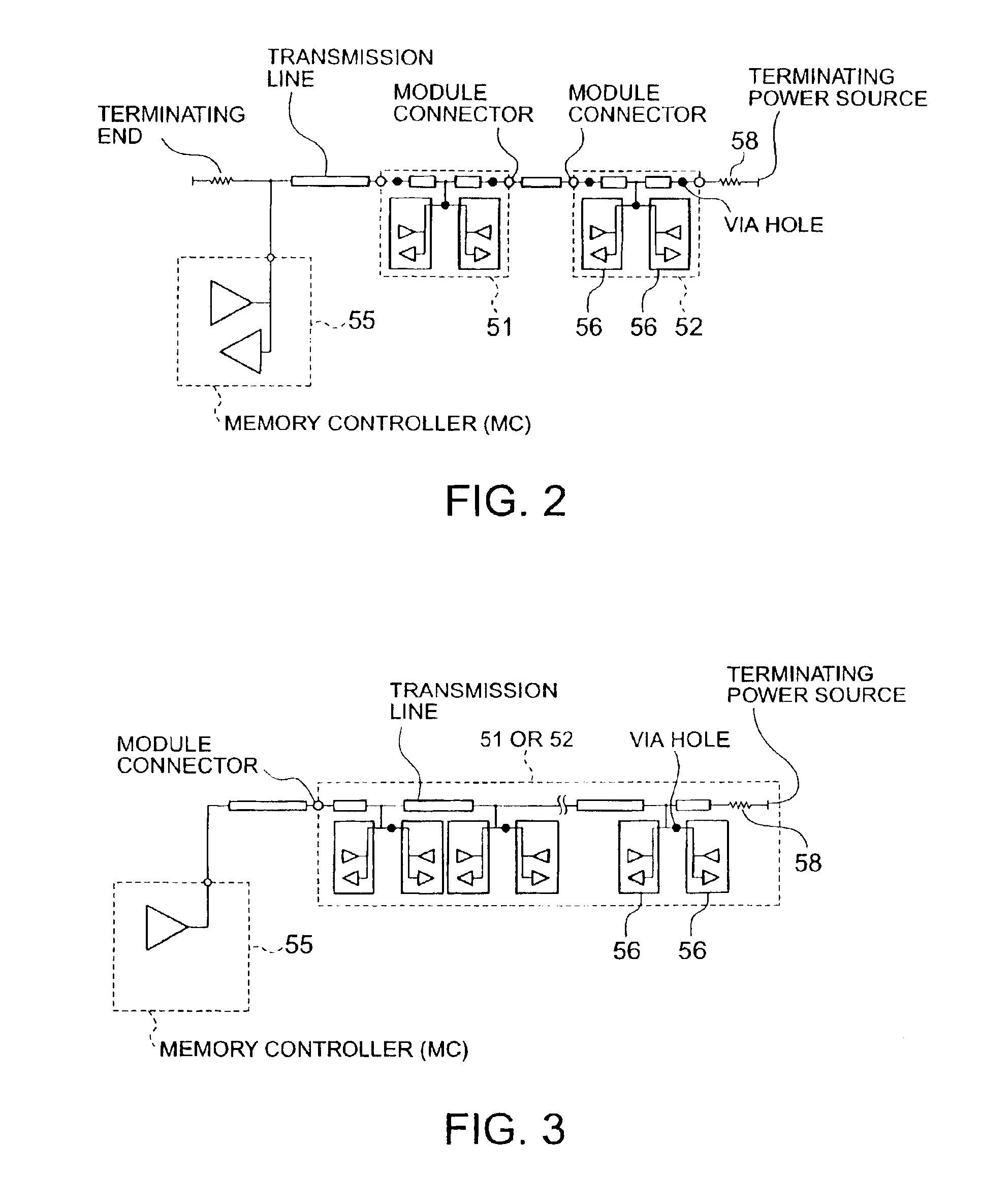
[0120]The MC 55 is connected to the DRAMs 56 on the modules 51 and 52 through dat...


PUM


Abstract

A memory system and a control method for the same enable stable operation at high frequencies without a radiant noise problem. In the memory system, a plurality of DRAMs is provided on each of a plurality of modules, and each DRAM is connected with a memory controller by data lines and clock lines. The clock lines have a topology exclusively applied to each module, while the data lines have a topology for connecting them to their associated DRAMs on each module. Command/address lines also have a topology similar to that of the clock lines. In this case, data signals supplied through the data lines and clock and command/address signals supplied through the clock lines and the command/address lines are transferred at different timings between the DRAMs and the memory controller. For this reason, the DRAMs and the memory controller are provided with circuits for matching the timings.

Description

BACKGROUND OF THE INVENTION[0001]1. Field of the Invention[0002]The present invention relates to a memory system including a semiconductor memory, such as a DRAM, and a control method for the same.[0003]2. Description of the Related Art[0004]As this type of memory system, there is one disclosed in Japanese Unexamined Patent Publication No. 2001-256772 (hereinafter referred to as “quoted example 1”). In quoted example 1, a clock signal supplied from a memory controller MC to each module is reproduced and buffered through a PLL circuit on the module before it is distributed to each DRAM on the module. Meanwhile, an address and command signal is buffered by a buffer on each module before it is distributed to each DRAM. A data signal is supplied from the MC to the DRAMs on each module in parallel.[0005]Quoted example 1 discloses a topology in which a data line on each module is not branched with respect to a data bus on a motherboard. This enables the operating frequency of a signal to ...

Claims


Application Information

Patent Timeline
IPC IPC(8): G11C7/10G11C7/00G11C7/22G11C11/406G06F12/00G06F13/16
CPCG11C7/1051G11C7/1066G11C7/1078G11C7/1087G11C7/109G11C7/22G11C7/222G11C11/406G11C2207/2254G11C11/40
Inventor MATSUI, YOSHINORI
Owner LONGITUDE SEMICON S A R L
Why Eureka
Try Eureka