Polishing method using an abrading plate

a technology of abrading plate and polishing plate, which is applied in the direction of manufacturing tools, abrasive surface conditioning devices, lapping machines, etc., can solve the problems of reducing the polishing rate, the inability to operate the self-stopping function, and the continual grinding of the surface, so as to achieve stable polishing rate, reduce the amount of surface removal, and reduce the effect of polishing ra

Inactive Publication Date: 2005-09-13
EBARA CORP
View PDF45 Cites 27 Cited by
  • Summary
  • Abstract
  • Description
  • Claims
  • Application Information

AI Technical Summary

Benefits of technology

[0021]A method is presented for polishing a semiconductor device wafer, having fine surface structure fabricated on a polishing surface, using an abrading plate. The method includes the conditioning steps of: dressing an abrading surface of the abrading plate so as to produce a roughened structure on the abrading surface; removing released particles attached to the roughened structure; and polishing the polishing surface with a conditioned abrading plate having a stabilized polishing rate generated by the foregoing steps. According to the method, the characteristic feature of the self-stopping function of the present abrading plate can be fully effective to be utilized in polishing the semiconductor device wafer.
[0022]Also, the present method of polishing of the semiconductor device wafer having fine structures fabricated on the surface includes a feature that an abrading surface of an abrading plate is dressed to a produce micro-rough surface, and released abrasive particles attached to the abrading surface are removed before pressing onto a surface of an object to be polished, so that the abrading surface has reached a stabilized condition to polish a blanket wafer (a wafer covered by an overall film) at a sufficiently low polishing rate. This procedure is effective in generating the self-stopping capability.
[0023]Also, the present method of polishing of the semiconductor device wafer having fine structures fabricated on the surface includes a feature that the additional surface removal is performed with an abrading plate using a liquid not containing any abrasive particles for a specific duration, followed by additional polishing using a slurry containing abrasive particles to the surface to be polished. A specific duration is a duration sufficient for the surface to be leveled by removing the high and low spots. According to this method, it enables the use of the same abrading plate to obtain additional surface removal by using a slurry containing a large amount of released abrasive particles. Because this polishing is carried out using a slurry containing a large amount of abrasive particles, surface removal can be achieved in a relatively short time to obtain a desired film thickness.
[0024]Also, the present method of polishing of the semiconductor device wafer having fine structures fabricated on the surface includes a feature that the additional surface removal is performed using an abrading plate and a liquid not containing any abrasive particles for a specific duration, followed by additional polishing using released abrasive particles being produced from concurrent dressing of the abrading plate. This method enables the use of the same abrading plate so that the released abrasive particles, being produced by carrying out dressing concurrently with the polishing by abrading plate, are used to obtain quick removal of the surface material, thereby raising the polishing rate. Therefore, it is not necessary to have additional facilities such as the polishing solution supply device so that a regular facility based on the abrading plate can be used to perform additional surface removal.
[0025]Also, the present method of polishing of the semiconductor device wafer having fine structures fabricated on the surface includes a feature that additional removal is performed using an abrading plate and a liquid not containing any abrasive particles for a specific duration, followed by additional polishing using a polishing cloth and a slurry containing abrasive particles. This method enables the use of the existing facility to carry out additional surface removal based on conventional slurry and polishing cloth.
[0026]When the abrasive surface of the abrading plate is relatively soft so that there is less danger of scratching the polishing surface of the wafer, first, polishing by the abrading plate is performed while supplying a liquid without containing abrasive particles (for example, pure water containing a surface-active agent), and second, finishing by soft cloth is performed while supplying pure water (or a chemical liquid not containing abrasive particles).

Problems solved by technology

If the abrasive particles are in excess or the binder material is insufficient, abrasive particles are easily self-generated (released), so that abrading continues even after a level surface has been produced, and the self-stopping function cannot operate.
If the amount of abrasive particles is insufficient or, binder material is in excess, abrasive particles are difficult to be self-generated (released) and the polishing rate is reduced so that polishing capacity is decreased.
In other words, too much porosity makes the abrading plate too soft and promotes generation of released particles while too little porosity makes the abrading plate too hard to discourage self-generation of freed particles (released).

Method used


Image

  • Polishing method using an abrading plate
  • Polishing method using an abrading plate
  • Polishing method using an abrading plate

Examples


first embodiment

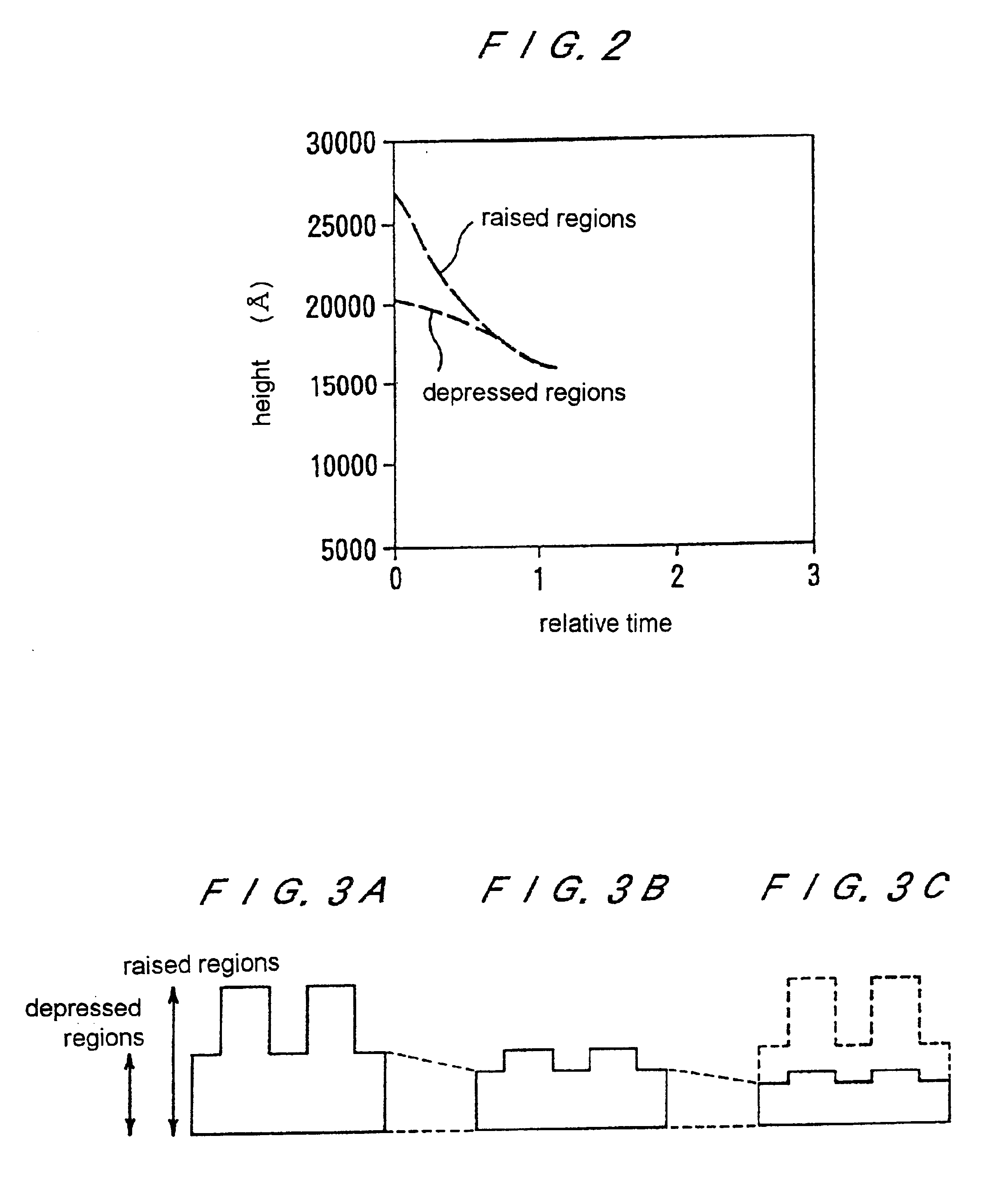
[0103]FIGS. 18A, 18B are schematic illustrations of the process of the present method. The first stage polishing is shown in FIG. 18A, and is based on the polishing using the abrading plate described above. This abrading plate has a self-stopping property that enables the reduction of the rate of material removal when the raised regions of the semiconductor device patterned wafer are preferentially eliminated and the irregularities are eliminated by polishing while supplying only water W from the nozzle 10. However, when it is necessary to control the film thickness to a certain value, this abrading plate is not suitable because further polishing does not remove the surface material, due to working of the self-stopping function.

[0104]For this reason, first, polishing time is controlled so as to recognize that the irregularities have been eliminated. Then, in the second stage polishing shown in FIG. 18B, additional polishing is carried out by replacing water with a polishing slurry c...

second embodiment

[0108]FIGS. 23A, 23B show the polishing method. FIG. 23A shows a second stage polishing apparatus used for the first stage polishing using the abrading plate, and FIG. 23B shows a polishing apparatus having a diamond dresser 16 added to the apparatus shown in FIG. 23A. Diamond dresser 16 comprises fine diamond particles of about #200 particle size embedded in the abrading surface of the abrading plate 15, and performs conditioning of the abrading plate 15 using water W. As illustrated, on one location on the surface of a rotating turntable 5, polishing of wafer W is carried out by the abrading plate, while, on the other location, dressing of the abrading plate is carried out by pressing the dresser 16 on the abrading surface of the abrading plate while supplying water W from the nozzle 10.

[0109]The first and second stage polishing in the second embodiment are controlled by switching a series of valves using the switching apparatus shown in FIG. 24 according to the flowchart shown in...

third embodiment

[0110]FIGS. 26A, 26B show the polishing method schematically, and FIG. 27 shows a plan view of the apparatus. A wafer 4 that has passed through the first stage polishing using the abrading plate 15 shown in FIG. 26A is transferred to a conventional CMP apparatus shown in FIG. 26B using a polishing cloth 6 and slurry containing abrasive particles through a conventional chemical and mechanical polishing process. This CMP operation can be carried out using a single conventional apparatus, but it may be used in a combined manner with the polishing apparatus comprising the abrading plate so that both may be used in a complementary manner. Namely, because of the self-stopping function of the abrading plate using water or chemical solution, surface material removal will not proceed after the irregularities are eliminated in the process of polishing even in a subsequent polishing process. On the other hand, since the polishing cloth of conventional chemical mechanical polishing has elastici...


PUM

PropertyMeasurementUnit
heightaaaaaaaaaa
heightaaaaaaaaaa
heightaaaaaaaaaa

Abstract

An abrading plate has a self-stopping capability such that when an object, such as a semiconductor wafer having a device structure that includes raised regions and depressed regions fabricated on the surface, is being polished, the raised regions are removed and polishing stops automatically. The abrading plate, to produce a flat and mirror polished surface on the an object, has abrasive particles having a chemical purity of not less than 90% and a particle size of not more than two micrometers, a binder material, and a given volume of porosity. A ratio of the abrasive particles and the binder material is not less than 1:0.5 by volume, and proportions of abrasive particles, a binder material and porosity are, respectively, not less than 10%, not more than 60% and 10-40% by volume. A surface is polished for a given duration with a liquid not containing abrasive particles so as to eliminate the raised regions and to obtain a flat surface. Additional surface removal is performed by supplying abrasive particles to the polishing interface to remove surface material uniformly from the entire surface.

Description

CROSS-REFERENCES TO RELATED APPLICATIONS[0001]This is a continuation-in-part of U.S. patent application Ser. No. 09 / 446,764 now U.S. Pat. No. 6,413,149, which is the national phase of PCT / JP99 / 02270, filed Apr. 28, 1999. This is also a continuation-in-part of U.S. patent application Ser. No. 09 / 276,153, filed Mar. 25, 1999 now abandoned.[0002]Priority is claimed on JP 10 / 134,432, filed Apr. 28, 1998, JP 10 / 150,546, filed May 14, 1998, and JP 100405 / 1998, filed Mar. 27, 1998.[0003]U.S. patent application Ser. No. 09 / 446,764, and thus PCT / JP99 / 02270, U.S. patent application 09 / 276,153, JP 10 / 134,432, JP 10 / 150,546, and JP 100405 are incorporated herein by reference.BACKGROUND OF THE INVENTION[0004]1. Technical Field[0005]The present invention relates to a method for polishing an object such as a semiconductor wafer using an abrading plate to obtain a flat and mirror finish.[0006]2. Background Art[0007]Recently, as the density of circuit integration in semiconductor devices becomes eve...

Claims


Application Information

Patent Timeline
Patent Type & Authority Patents(United States)
IPC IPC(8): B24B1/00B24B37/04B24B37/24B24B53/017B24D3/32H01L21/304
CPCB24B37/042B24B37/245B24B53/017B24D3/32H01L21/31053H01L21/3212
Inventor WADA, YUTAKAHIYAMA, HIROKUNIHIROKAWA, KAZUTOMATSUO, HISANORI
Owner EBARA CORP
Why Eureka
Try Eureka