Method and apparatus for detecting pattern defects

a pattern defect and inspection method technology, applied in the direction of optically investigating flaws/contamination, semiconductor/solid-state device testing/measurement, instruments, etc., can solve the problems of low lighting efficiency, difficult correction of chromatic aberration of optical systems used for pattern inspection, enhancement and attenuation of light flux, etc., to achieve uniform illumination of samples, high accuracy of inspection, and high reliability of pattern defect inspection

Inactive Publication Date: 2005-09-13
HITACHI LTD
View PDF15 Cites 17 Cited by
  • Summary
  • Abstract
  • Description
  • Claims
  • Application Information

AI Technical Summary

Benefits of technology

[0012]The present invention has the object of providing an optical system which is able to uniformly illuminate a sample without being affected by variations in the thickness of a transparent thin film formed over the surface of the...

Problems solved by technology

A larger size lamp with higher power must therefore be used to obtain a sufficient light intensity, but this results in the problem of lower lighting efficiency.
Yet another problem is that correcting the chromatic aberration of optical systems used for pattern inspection is difficult due to the wide spectral bandwidth.
However, these exci...

Method used


Image

  • Method and apparatus for detecting pattern defects
  • Method and apparatus for detecting pattern defects
  • Method and apparatus for detecting pattern defects

Examples


Embodiment Construction

[0043]Preferred embodiments of a high-resolution optical system and a pattern defect inspection apparatus of the present invention will be described in detail with reference to the accompanying drawings.

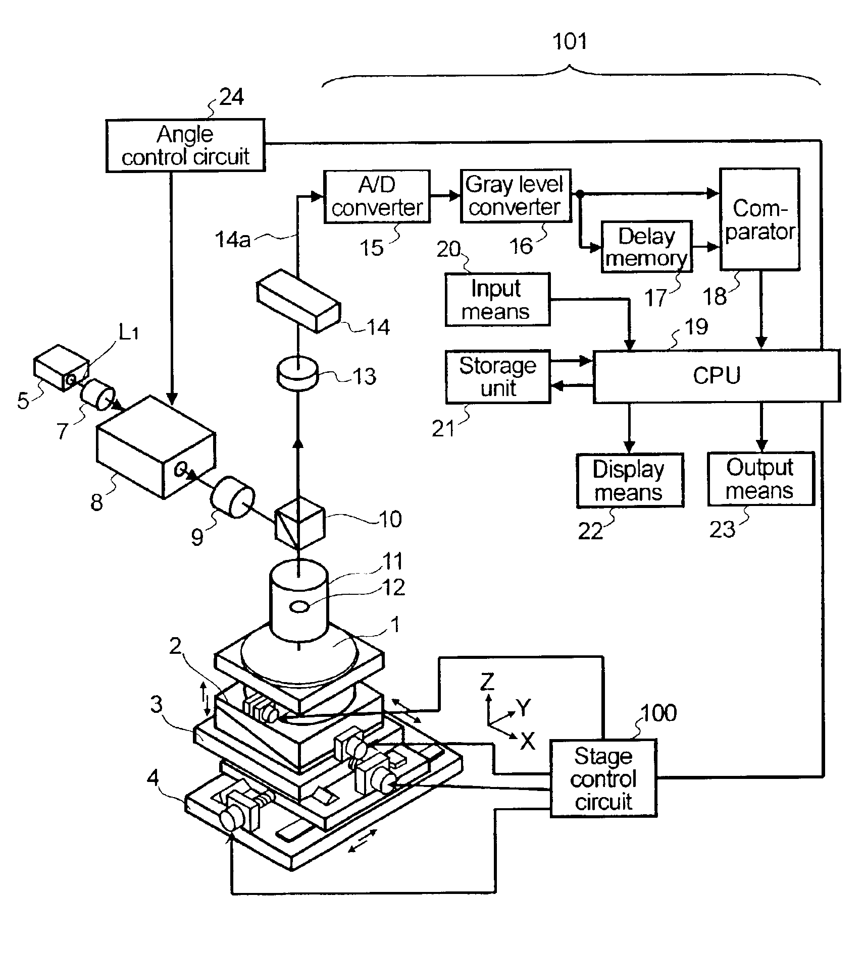
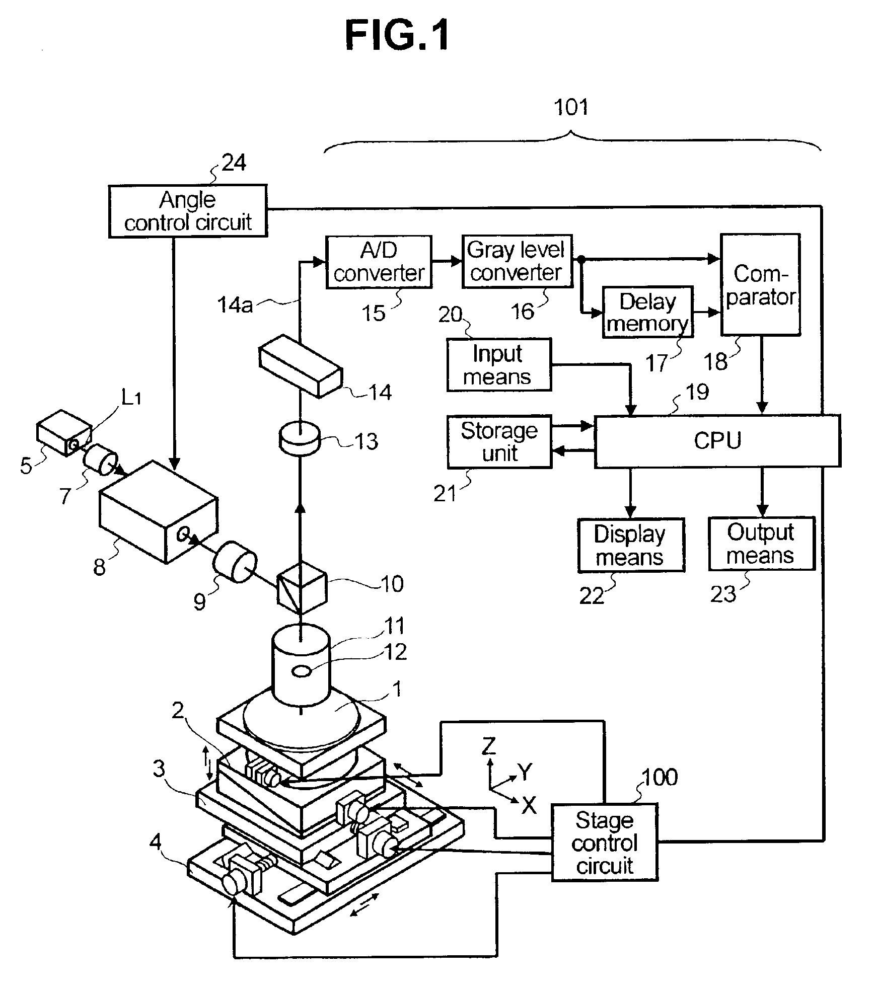
[0044]FIG. 1 is a schematic diagram showing a pattern defect inspection apparatus representing a first embodiment of the present invention. Reference numeral 1 in FIG. 1 denotes a sample constituted, for example, by a semiconductor wafer (device under test) on which there is fabricated a circuit pattern to be inspected. The sample 1 is placed and held on a Z stage 2 (by means, for example, of a vacuum chuck or electrostatic chuck that is not shown in the drawing) that moves in the Z direction and rotates. A Y stage 4 and an X stage 3 can be independently moved to any desired position under control from a stage control circuit 100. The position of each stage is constantly detected by a length measuring device or position sensor (not shown in the drawing). The detected position data, i...


PUM


Abstract

A method and apparatus for detecting pattern defects which includes annularly scanning of a laser beam emitted from a laser light source on a pupil of an objective lens, illuminating the scanned laser beam, through the objective lens, onto a sample on which there is formed a pattern coated with an optically transparent thin film, acquiring an optical image of the illuminated sample, and processing the acquired image to find defects in the pattern. The annular scan diameter of the laser beam is determined based on the thickness of the optically transparent thin film.

Description

BACKGROUND OF THE INVENTION[0001]The present invention relates to pattern defect inspection methods and apparatus using a laser beam as illumination light, mainly for inspecting and observing micro pattern defects or foreign matter contamination occurring in manufacturing processes for semiconductor devices and flat panel displays.[0002]Circuit patterns tend to continually become finer and smaller as semiconductor devices become more highly integrated. Smaller and finer circuit patterns have spurred a demand for higher resolution when inspecting for defects of circuit patterns that have been formed on semiconductor wafers by photolithographic processes using photomasks or reticles. One technique for enhancing resolution when detecting pattern defects involves the use of illumination light on shorter wavelengths from visible light to ultraviolet light. Mercury lamps and xenon lamps, for example, have been conventionally used as illumination light sources, while only the required wave...

Claims


Application Information

Patent Timeline
IPC IPC(8): G01N21/88G01N21/956G01B11/30H01L21/66
CPCG01N21/95684
Inventor YOSHIDA, MINORUUTO, SACHIOMAEDA, SHUNJINAKATA, TOSHIHIKO
Owner HITACHI LTD
Why Eureka
Try Eureka