
Multi step electrodeposition process for reducing defects and minimizing film thickness

a multi-step, film-thickening technology, applied in the direction of semiconductor devices, printed circuits, electrical equipment, etc., can solve the problems of large overburden, high cost and time-consuming, and the thickness of copper material deposited on the surface of the substrate,

Active Publication Date: 2005-09-20
NOVELLUS SYSTEMS
View PDF11 Cites 22 Cited by
  • Summary
  • Abstract
  • Description
  • Claims
  • Application Information

AI Technical Summary

Problems solved by technology

In the prior art, however, after performing the material deposition to fill such features or cavities, a variation in the thickness of the deposited copper material inevitably occurs on the surface of the substrate.
However, the planarization and the removal of the large overburden resulting from the conventional deposition methods is expensive and time consuming.
Furthermore, large variations on the non-planar surface of the overburden result in defects such as dishing and erosion, after the overburden removal and planarization steps.

Method used


Image

  • Multi step electrodeposition process for reducing defects and minimizing film thickness
  • Multi step electrodeposition process for reducing defects and minimizing film thickness
  • Multi step electrodeposition process for reducing defects and minimizing film thickness

Examples


Embodiment Construction

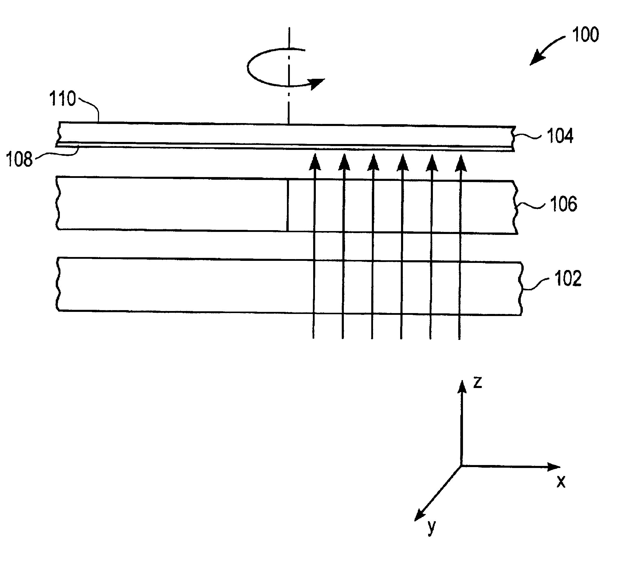
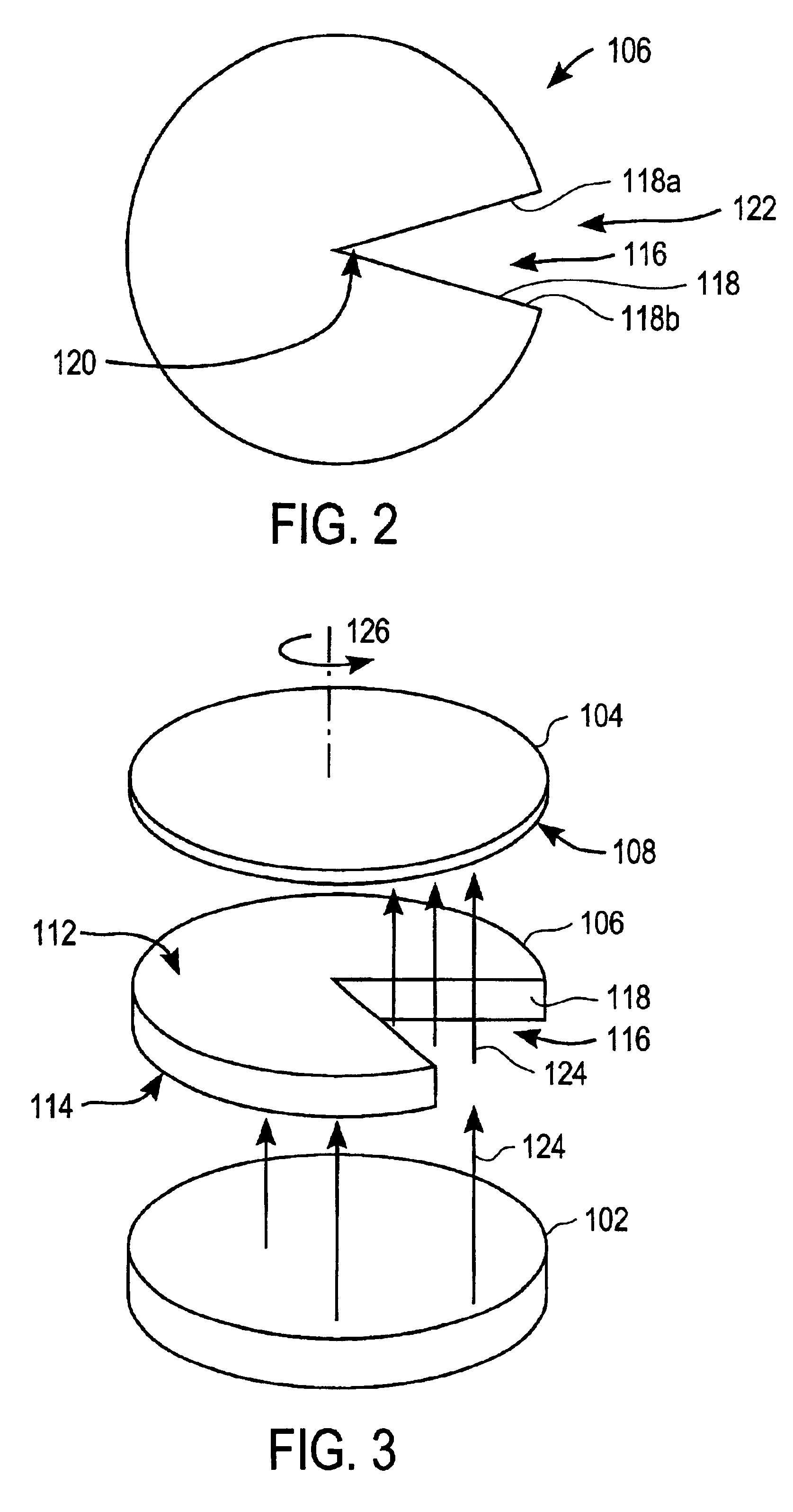
[0023]Reference will now be made to the drawings wherein like numerals refer to like parts throughout. An example of a planar electro deposition-polishing apparatus that can be used to practice the present invention is schematically shown in FIGS. 1-3. It should be noted that, in this application, process of electroetching, electropolishing, electrochemical etching are all used to refer to the process where a voltage is applied to a coating on a substrate in an electrolyte to remove part or all of the coating.

[0024]Descriptions of various methods and apparatus for electrodeposition of planar films can be found in the following patent and pending application, all commonly owned by the assignee of the present invention: U.S. Pat. No. 6,176,992 entitled “Method and Apparatus for Electrochemical Mechanical Deposition,” U.S. application Ser. No. 09 / 740,701 entitled “Plating Method and Apparatus that Creates a Differential Between Additive Disposed on a Top Surface and a Cavity Surface of...


PUM

PropertyMeasurementUnit
Electrical conductoraaaaaaaaaa
Widthaaaaaaaaaa
Depthaaaaaaaaaa

Abstract

The present invention relates to a method for forming a planar conductive surface on a wafer. In one aspect, the present invention uses a no-contact process with electrochemical deposition, followed by a contact process with electrochemical mechanical deposition.

Description

[0001]This application is related to and claims the benefit of and priority to U.S. Provisional Application No, 60 / 306,758 filed on Jul. 20, 2001 entitled “Multi Step Electrodeposition Process For Reducing Defects and Minimizing Film Thickness.”BACKGROUND OF THE INVENTION[0002]1. Field of the Invention[0003]The present invention generally relates to semiconductor processing technologies and, more particularly, to an electrodepositing process that deposits thin and planar layers.[0004]2. Description of the Related Art[0005]Conventional semiconductor devices generally include a semiconductor substrate, usually a silicon substrate, and a plurality of sequentially formed dielectric interlayers such as silicon dioxide and conductive paths or interconnects made of conductive materials. The interconnects are usually formed by filling a conductive material in trenches etched into the dielectric interlayers. In an integrated circuit, multiple levels of interconnect networks laterally extend ...

Claims


Application Information

Patent Timeline
IPC IPC(8): C25D5/02C25D5/22C25D7/12C25D5/00H01L21/02H01L21/70H01L21/288H01L21/768
CPCC25D5/02C25D5/22H01L21/2885H01L21/7684H01L21/76877C25D7/123C25D5/611
Inventor BASOL, BULENT M.UZOH, CYPRIAN E.TALIEH, HOMAYOUN
Owner NOVELLUS SYSTEMS
Learn More