Sample electrification measurement method and charged particle beam apparatus

a technology of electrification measurement and charge beam, which is applied in the direction of mechanical measurement arrangements, mechanical roughness/irregularity measurements, instruments, etc., can solve the problems of magnification fluctuations, measurement errors, and deviation of the focus of the charged particle beam, so as to reduce or eliminate measurement errors or magnification fluctuations.

Inactive Publication Date: 2005-09-20
HITACHI LTD
View PDF13 Cites 67 Cited by
  • Summary
  • Abstract
  • Description
  • Claims
  • Application Information

AI Technical Summary

Benefits of technology

[0009]A first object of the present invention is to provide a device and method for detecting the characteristic electrostatic charge state of the sample without having to also measure the electrostatic charge at each measurement point.
[0010]A second object of the present invention is to provide a method ideal for reducing or eliminating measurement errors or fluctuations in magnification due to electrostatic charges, a magnification adjustment method, and a device to implement these methods.

Problems solved by technology

Another possible cause is residual electrical charges from etching that uses plasma.
These residual electrostatic charges remaining on the sample can cause the focus of the charged particle beam to deviate and are a cause of magnification fluctuations and measurement errors in the charged particle beam device.
However, the technology disclosed in JP-A No. 176285 / 1995 has the following problems.
A long time is therefore needed to measure a wafer and this delay caused productivity to drop.
Other problems also still unresolved included errors in controlling the magnification, etc.
In the method disclosed in JP-A No. 52642 / 2001, using electrometers installed within a vacuum, the electrostatic electrical potential cannot be measured without moving to the measurement point so a long time was required to make a measurement at one point.
Another problem is that when a breakdown occurred, the charged particle and stage in the vacuum unit has to be exposed to the outside air so that maintenance of the equipment is difficult.
Yet another problem is that the multiple electrometers have to be adjusted to constantly provide the same output.

Method used


Image

  • Sample electrification measurement method and charged particle beam apparatus
  • Sample electrification measurement method and charged particle beam apparatus
  • Sample electrification measurement method and charged particle beam apparatus

Examples


first embodiment

(First Embodiment)

[0038]The embodiments of the present invention are described next while referring to the drawings. The example in the embodiment was described as using a scanning electron microscope (SEM). However, the present invention is not limited to this and other charged particle beam devices such as ion beam irradiation devices can be used. The example in the present embodiment also describes detecting secondary electrons and / or reflected electrons which are one type of charged particle. However, the present invention is not limited to this and may detect other charged particles such as secondary ions, etc.

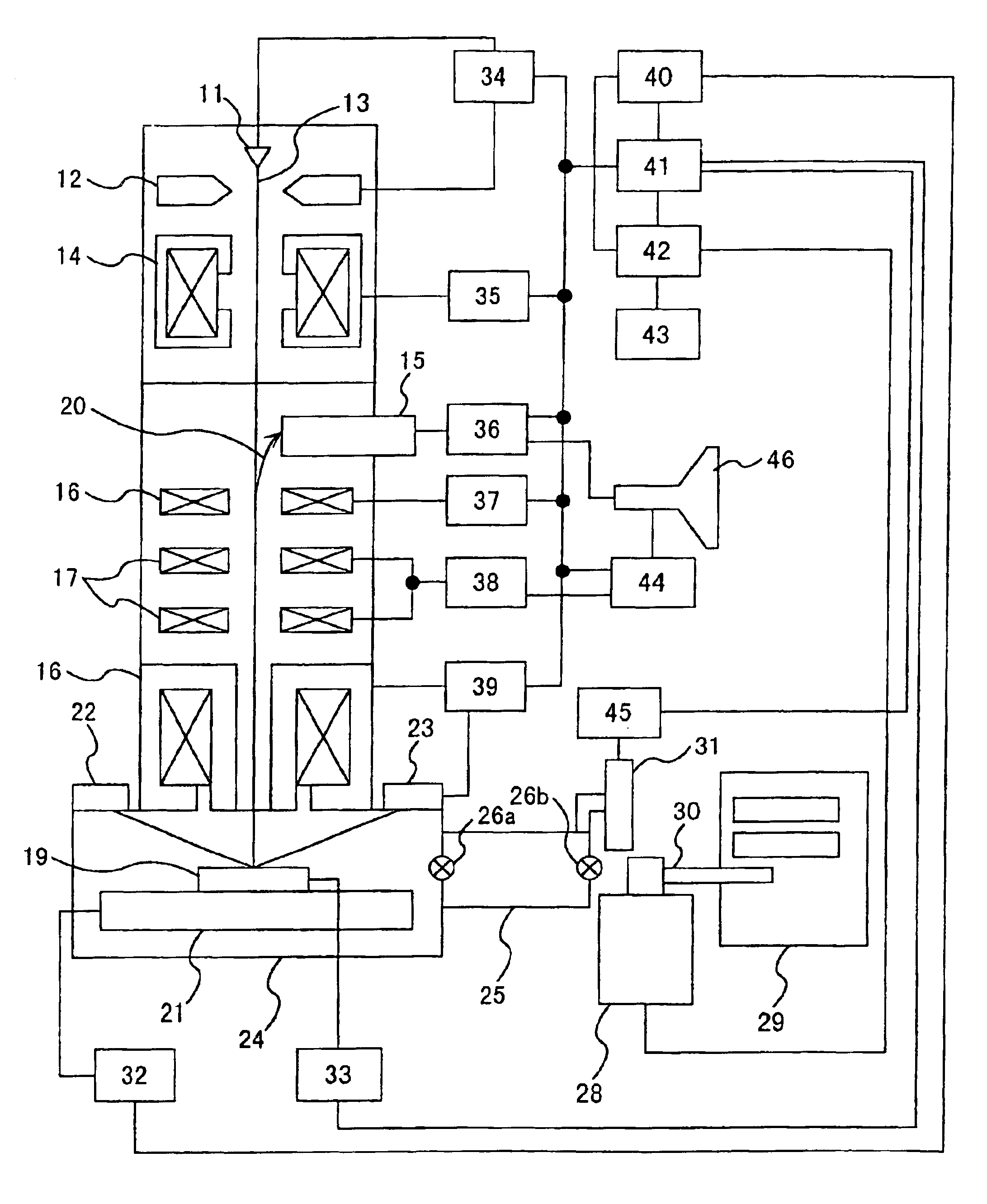
[0039]FIG. 1 shows the overall structure of the present invention. An integrated controller 42 controls the overall device via the charged particle optical system controller 41, stage controller 40, and wafer conveyor 28, based on the observation position information, wafer information and acceleration voltage of the charged particle entered by the operator from the user ...

second embodiment

(Second Embodiment)

[0061]In view of the problems in making accurate tests and measurements in particular when different electrostatic charge phenomenon occur in the sample (semiconductor wafer, etc.), the embodiment described next relates to a device and method allowing highly precise testing and measurement even when different electrostatic charge phenomenon.

[0062]In a charged particle beam device, output information from a secondary charged particle detector is synchronized with the scanning by the charged particle beam and reproduced on an image display device as described above. The ratio of distance A between two points on the scanned image on the CRT (or display device) versus the distance a between two points on the sample, is the observation magnification MSEM.

MSEM=A / a

[0063]The distance a between two points on the sample is usually in inverse proportion to the observation magnification MSEM since the screen on the display device is a fixed size. By therefore measuring the di...

third embodiment

(Third Embodiment)

[0100]The localized electrostatic voltage ΔVs varies the optical magnification Mobj of the objective lens as described using FIG. 11. The electrostatic voltage ΔVs is localized due to electron beam irradiation so there is almost no effect on the excitation current I6. Regardless of this, the localized electrostatic voltage ΔVs forms a minute electrostatic lens 108b. This lens causes the track 101a of the primary electron beam to be deflected by the global (wide area) electrostatic charge so as to concentrate onto the track 101b and make the optical magnification Mobj greatly fluctuate as described in the previous embodiment.

[0101]Yet another method is described next for making accurate tests and measurements that are otherwise difficult due to different, overlapping electrostatic phenomenon.

[0102]The present embodiment proposes a method for correcting the magnification fluctuation using the localized electrostatic voltage ΔVs and calculating the correct optical mag...


PUM

PropertyMeasurementUnit
voltageaaaaaaaaaa
voltageaaaaaaaaaa
voltageaaaaaaaaaa

Abstract

The present invention has the object of providing a charged particle beam irradiation method ideal for reducing the focus offset, magnification fluctuation and measurement length error in charged particle beam devices.To achieve these objects, a method is disclosed in the invention for measuring the electrical potential distribution on the sample with a static electrometer while loaded by a loader mechanism. Another method is disclosed for measuring the local electrical charge at specified points on the sample, and isolating and measuring the wide area electrostatic charge quantity from those local electrostatic charges. Yet another method is disclosed for correcting the measurement length value or magnification based on fluctuations found by measuring the amount of electrostatic charge at the specified points under at least two charged particle optical conditions, and then using a charged particle beam to measure fluctuations in measurement dimensions occurring due to fluctuations in the electrostatic charge at the specified locations.

Description

TECHNICAL FIELD[0001]The present invention relates to a charged particle beam device and relates in particular to a measurement method and device thereof for inspecting or measuring the dimensions and shape of a pattern formed on a sample piece.BACKGROUND ART[0002]The greater scale of integration and miniaturization of semiconductor devices in recent years has resulted in many diverse patterns being formed on the wafer and makes it ever more important to evaluate and measure the dimensions and shapes of these patterns. How fast these measurement points can be detected is critical for quickly and automatically testing the numerous measurement points. During fast detection of measurement points, it is necessary to focus on the pattern after shifting to the measurement point and to also set the desired magnification (scale) for observing that point.[0003]In charged particle optical systems, the conditions for focusing on the wafer are determined by the acceleration voltage of the charg...

Claims


Application Information

Patent Timeline
Patent Type & Authority Patents(United States)
IPC IPC(8): H01J37/02H01J37/28H01J37/21G01N23/00G01Q30/06G01Q30/18G01Q30/20G21K7/00
CPCG01N23/2251H01J37/21H01J37/244H01J37/265H01J37/28H01J2237/2817H01J2237/216H01J2237/244H01J2237/24564H01J2237/24592H01J2237/2594H01J2237/0041
Inventor EZUMI, MAKOTOOSE, YOICHIIKEGAMI, AKIRATODOKORO, HIDEOISHIJIMA, TATSUAKISATO, TAKAHIROFUKAYA, RITSUOASAO, KAZUNARI
Owner HITACHI LTD
Why Eureka
Try Eureka