Semiconductor device with capacitor formed around contact hole

a technology of capacitors and semiconductors, applied in the field of semiconductor devices, can solve the problems of reducing the aperture ratio of the ips liquid crystal display device and difficult to ensure a sufficient storage capacitance, and achieve the effect of high aperture ratio

Inactive Publication Date: 2005-09-27
SEMICON ENERGY LAB CO LTD
View PDF34 Cites 58 Cited by
  • Summary
  • Abstract
  • Description
  • Claims
  • Application Information

AI Technical Summary

Benefits of technology

[0013]An object of the present invention disclosed in this specification is to provide a technique for solving the conventional problems stated above. Namely, an object of the present invention is to provide a proposal of a method of forming a storage capacitor in an IPS liquid crystal display device, and to provide a technique of forming a pixel region having a high aperture ratio.

Problems solved by technology

The electrode surface area necessary for these electrodes therefore reduces the aperture ratio of the IPS liquid crystal display device.
In addition, if the wirings and the electrodes are made minuter in order to increase the aperture ratio, then it becomes difficult to ensure a sufficient storage capacitance.

Method used


Image

  • Semiconductor device with capacitor formed around contact hole
  • Semiconductor device with capacitor formed around contact hole
  • Semiconductor device with capacitor formed around contact hole

Examples


embodiment 1

[Embodiment 1]

[0088]Embodiment 1 of the present invention is explained by using FIGS. 4A to 8. A method of manufacturing a pixel portion and a driver circuit in order to drive the pixel portion at the same time, and on the same substrate, is explained. Note that in order to simplify the explanation, a CMOS circuit, a basic circuit for circuits such as a shift register circuit and a buffer circuit, and an n-channel TFT which forms a sampling circuit, are shown in the figures.

[0089]It is preferable to use a quartz substrate or a silicon substrate as a substrate 401 in FIG. 4A. A quartz substrate is used in embodiment 1. In addition, a substrate such as a metallic substrate or a stainless steel substrate on which an insulating film is formed on the surface may also be used. In embodiment 1, a heat resistance capable of withstanding 800° C. or greater is required, and provided that it can fulfill this condition, any substrate may be used.

[0090]A semiconductor film 402 containing an amor...

embodiment 2

[Embodiment 2]

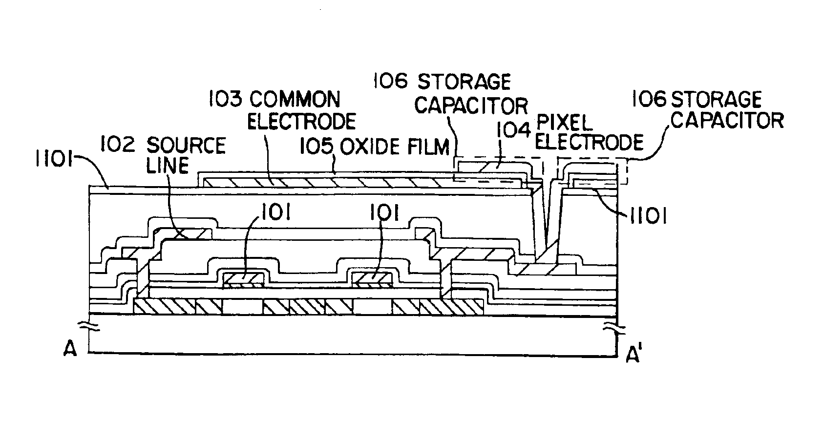
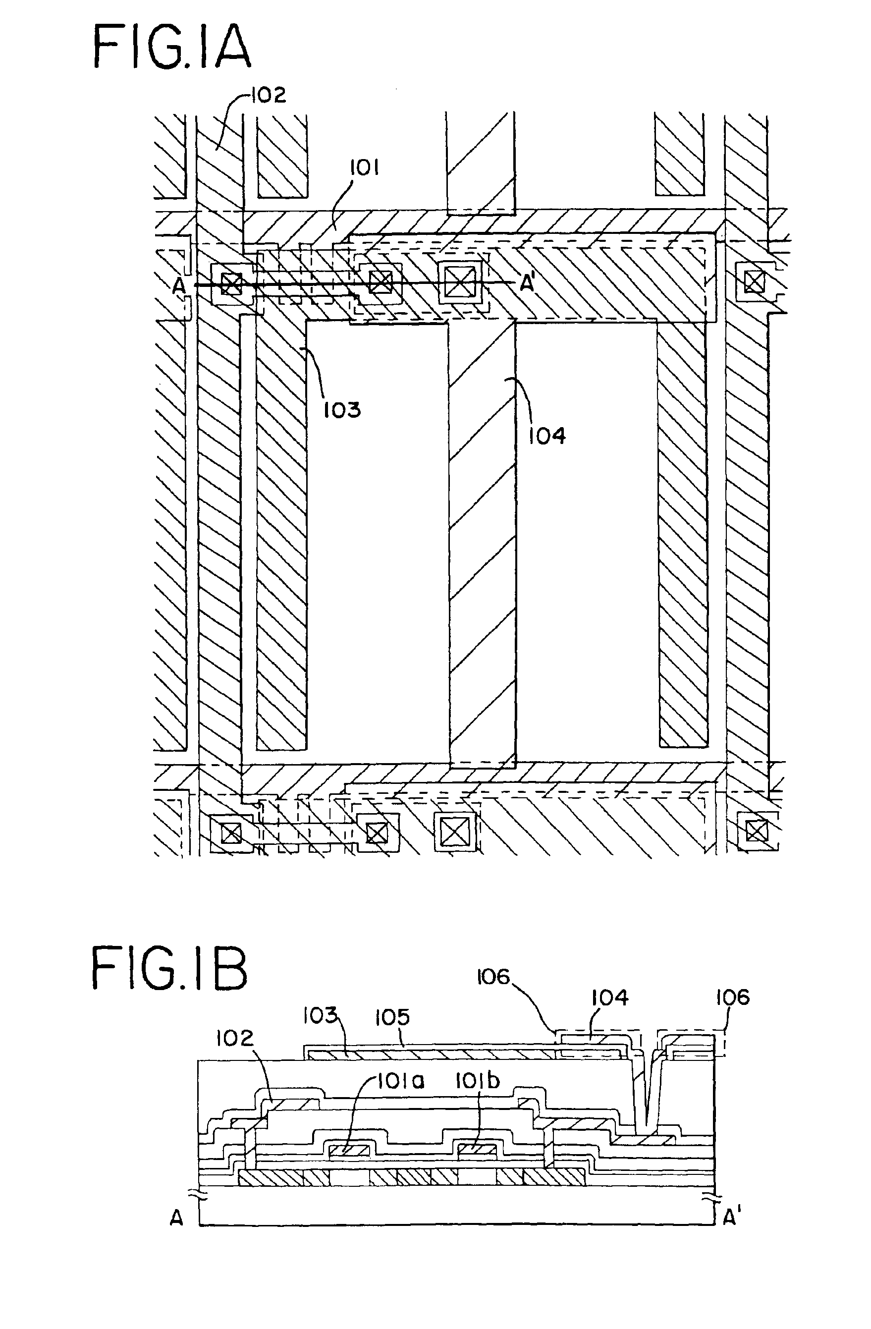
[0189]FIGS. 11A to 11C are used in embodiment 2 to explain a case of a pixel portion structure which differs from that of embodiment 1. Note that the basic structure is the same structure as that shown in FIG. 1B, and therefore only points of difference are explained. Consequently, the same symbols are used for identical portions.

[0190]FIG. 11A is a cross sectional diagram of the pixel portion of embodiment 2, and is an example of forming a buffer layer 1101 between an interlayer insulating film (organic resin film) and the common electrode 103. An insulating film containing silicon with a thickness of between 10 and 100 nm (preferably between 30 and 50 nm) is used as the buffer layer 1101. However, in forming the buffer layer on the organic resin film, there is a problem of degasification from within the resin film if it is exposed to a vacuum, and therefore it is preferable to use an insulating film which can be formed by sputtering.

[0191]A 50 nm thick silicon oxide ...

embodiment 3

[Embodiment 3]

[0198]In embodiment 3, a case of the shape of the common electrode of the pixel portion differing from that of embodiment 1 is explained using FIG. 12 and FIG. 13. Note that the basic structure is the same structure as that shown in FIG. 1A, and therefore only points of difference are explained. Consequently, the same symbols are used for identical portions.

[0199]In order to set the common electrode to a common electric potential (an intermediate electric potential of the image signal sent as data) in embodiment 3, a common electrode 1201 with a shape connected to each of the common electrodes is formed. By then electrically connecting an electric power supply line for imparting a common electric potential to the common electrode 1201, outside of the pixel portion, the common electrode 1201 can be maintained at the common electric potential. Note that when the common electrode 1201 is used, the step of cutting apart after anodic oxidation can be omitted, and therefore ...


PUM

PropertyMeasurementUnit
current densityaaaaaaaaaa

Abstract

A method of forming a storage capacitor in an IPS liquid crystal display device is proposed, and a technique of forming a pixel region having a high aperture ratio is provided. An anodic oxidation process at an applied voltage/voltage supply time ratio of 11 V/min is performed for insulating films used in each circuit of an electro-optical device, typically an IPS method LCD, in particular for the surface of a common electrode formed on a resin film. The amount of formation of the extra anodic oxide film can be reduced by covering with an anodic oxide film, and a liquid crystal display device with high reliability and having an electrode with superior adhesion can be manufactured.

Description

[0001]This application is a divisional of U.S. application Ser. No. 09 / 573,314, filed on May 18, 2000 now U.S. Pat. No. 6,630,977BACKGROUND OF THE INVENTION[0002]1. Field of the Invention[0003]The present invention relates to a semiconductor device having a circuit composed of a thin film transistor (hereafter referred to as TFT), and to a method of manufacturing thereof. For example, the present invention relates to an electro-optical device, typically a liquid crystal display panel, and to electronic equipment loaded with that kind of electro-optical device as a part.[0004]Note that, throughout this specification, the term semiconductor device specifies devices in general which function by utilizing semiconductor characteristics, and that electro-optical devices, semiconductor circuits, and electronic equipment are all semiconductor devices.[0005]2. Description of the Related Art[0006]Techniques of forming thin film transistors (TFTs) using a semiconductor thin film (with a thickn...

Claims


Application Information

Patent Timeline
Patent Type & Authority Patents(United States)
IPC IPC(8): G02F1/13G02F1/1343G02F1/1362H01L21/336H01L29/786H01L21/02H01L21/70H01L29/66H01L27/12H01L21/84G02F1/1339H01L21/77H01L27/13
CPCG02F1/134363G02F1/136213G02F1/136227G02F1/1368H01L29/66757H01L29/78621H01L29/78675H01L27/1255H01L27/124H01L27/1248G02F1/13394G02F1/13454H01L29/786
Inventor YAMAZAKI, SHUNPEIHIRAKATA, YOSHIHARUMURAKAMI, SATOSHI
Owner SEMICON ENERGY LAB CO LTD
Why Eureka
Try Eureka