Wafer fabrication data acquisition and management systems

a data acquisition and management system technology, applied in the direction of electrical programme control, program control, instruments, etc., can solve the problems of inconvenient data acquisition, electrical short, and inconvenient data acquisition, so as to improve process control, improve data transfer capacity, and improve quality. the effect of yield and cost reduction

Inactive Publication Date: 2005-10-04
APPLIED MATERIALS INC
View PDF59 Cites 306 Cited by
  • Summary
  • Abstract
  • Description
  • Claims
  • Application Information

AI Technical Summary

Benefits of technology

[0016]Accordingly, a need exists for methods and techniques which provide improved data transfer capacity between a tool and a host computer, as well as improved process control, quality, yield and cost reduction. Also, there is a need to integrate wafer fab equipment time states

Problems solved by technology

For example, if there is an error in the overlay or alignment of etch masks for interconnects in adjacent IC layers, the resulting interconnects are not in their proper design location.
This can result in interconnects which are packed too closely, forming electrical short defects between these interconnects.
It is also well known that two different processing problems can have a cumulative effect.
For example, a misalignment of interconnect etch masks which is not extensive enough to result in an electrical short, can still contribute to causing an electrical short if the process is slightly out of specification for allowing (or not detecting) particulate contamination having a particle size which would not have caused an electrical short if the interconnect masks had been in good alignment.
When possible, yield problems are traced back to specific product or processing problems or defec

Method used


Image

  • Wafer fabrication data acquisition and management systems
  • Wafer fabrication data acquisition and management systems
  • Wafer fabrication data acquisition and management systems

Examples


Embodiment Construction

[0037]While describing the invention and its embodiments, certain terminology will be utilized for the sake of clarity. It is intended that such terminology includes the recited embodiments as well as all equivalents.

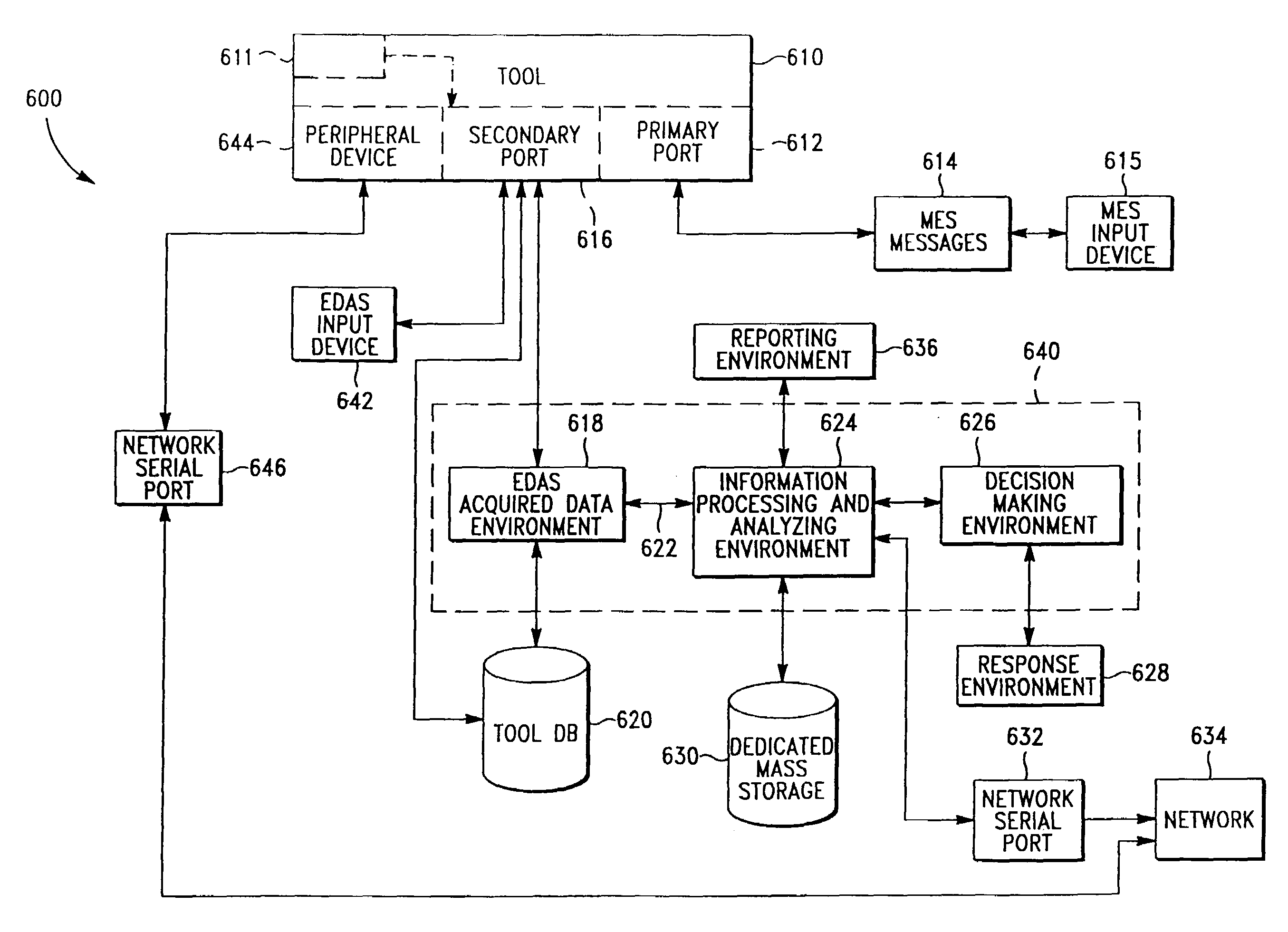
[0038]One embodiment of the invention, schematically illustrated in FIG. 6, shows a semiconductor processing device 600, employing an EDAS (enhanced data acquisition system) of the present invention. The novel EDAS is adapted for monitoring, i.e. observing, analyzing and reporting, semiconductor wafer or IC (integrated circuit) fabricating or processing tools, hereinafter referred to as tools. These tools include wafer fab chambers such as etch and deposition chambers, as well as wafer and wafer cassette handling equipment. The novel EDAS includes: (1) a DB (database) for storing information concerning equipment, processes and wafer data, (2) software adapted for performing data acquisition or collection, SPC analysis and historical reporting, and (3) a UI (user interfa...


PUM


Abstract

The present invention provides a semiconductor processing device (800) including a tool (802) having one or more sensors, a primary data communication port (804) and a secondary data communication port (806). A sensor data acquisition subsystem (808) acquires sensor data from the tool via the secondary port (806). The data acquisition subsystem (808) acquires MES operation messages via the primary port (804). Sensor data are communicated to a sensor processing unit (828) of a sensor data processing subsystem (810). The sensor processing unit (828) processes and analyzes the sensor data. Additionally, the processing unit (828) can be adapted for making product or processing related decisions, for example activating an alarm if the process is not operating within control limits. In another embodiment, the present invention provides a method and apparatus for processing data from a wafer fab facility (1000) including a plurality of tools (1004–1010) each having a primary data communication port (1012–1018) and a secondary data communication port (1042–1048).

Description

FIELD OF THE INVENTION[0001]The present invention relates to devices, techniques and methods for semiconductor processing.BACKGROUND OF THE INVENTION[0002]A semiconductor device such as an IC (integrated circuit) generally has electronic circuit elements such as transistors, diodes and resistors fabricated integrally on a single body of semiconductor material. The various circuit elements are connected through conductive connectors to form a complete circuit which can contain millions of individual circuit elements. Integrated circuits are typically fabricated from semiconductor wafers in a process consisting of a sequence of processing steps. This process, usually referred to as wafer fabrication or wafer fab, includes such operations as oxidation, etch mask preparation, etching, material deposition, planarization and cleaning.[0003]A summary of an aluminum gate PMOS (p-channel metal oxide semiconductor transistor) wafer fab process 40 is schematically shown in FIG. 1, illustrating...

Claims


Application Information

Patent Timeline
IPC IPC(8): G05B19/042G05B19/04H01L21/302H01L21/02H01L21/205H01L21/3065
CPCG05B19/042H01L21/00
Inventor CORDOVA, SHERRYDOYLE, TERRY L.KROUPNOVA, NATALIALOBOVSKI, EVGUENILOUNEVA, INNALYON, RICHARD C.NISHIMURA, YUKARINOLET, CLARIREISS, TERRYTOH, WOON YOUNGWILMER, MICHAEL E.
Owner APPLIED MATERIALS INC
Why Eureka
Try Eureka