High voltage withstanding semiconductor device

a semiconductor and high-voltage technology, applied in the direction of semiconductor devices, electrical devices, transistors, etc., can solve the problems of reducing the withstanding capacity, reducing the resistance to short circuiting, and increasing the problem of oscillation due to the feedback capacitan

Inactive Publication Date: 2005-10-11
MITSUBISHI ELECTRIC CORP
View PDF17 Cites 43 Cited by
  • Summary
  • Abstract
  • Description
  • Claims
  • Application Information

AI Technical Summary

Benefits of technology

[0029]In order to gain the effects of the invention disclosed in Japanese Patent Laying-Open No. 9-331063, it is essential for (2×dx) / Pi to be small. Here, (2×dx) / Pi is a ratio of p-type body region 102 that is connected to the emitter potential E in a cell.
[0030]In addition, in Japanese Patent Laying-Open No. 7-50405 that discloses an invention that is similar to the invention according to Japanese Patent Laying-Open No. 9-331063, it is cited as a requirement that (Pi+dy) / (2×dx) is no less than five when the difference between the depth of a trench and the depth of a p-type body region is dy. Here, dx is the width of a p-type body region that is connected to the emitter potential E and that corresponds to one channel of a MOS transistor.
[0031]That is to say, in the invention according to Japanese Patent Laying-Open No.9-331063, the requirement for the lowering of the saturation voltage specifies that Pi / dx is large, irregardless of dy and does not specify that conductive layer 105b, which fills in trench 101b for an emitter, becomes of the emitter potential.
[0032]FIG. 56 is a diagram showing an equivalent circuit of an IGBT. In reference to FIG. 56, in the inventions according to Japanese Patent Laying-Open No.7-50405 and Japanese Patent Laying-Open No.9-331063, Pi / dx is increased so that Pi is increased in reference to dx, which is restricted because of a microscopic processing limitation. Therefore, a portion of a MOS transistor structure formed in a unit area is reduced. Accordingly, the voltage drop Vmos in the MOS transistor Tr portion becomes greater than that in the structure of FIG. 52 wherein there is no emitter trench.
[0033]On the other hand, in the inventions according to Japanese Patent Laying-Open No.7-50405 and Japanese Patent Laying-Open No.9-331063, the carrier concentration in a region in the vicinity of the emitter side of n-type substrate 101 rises, as shown in Japanese Patent Laying-Open No. 7-50405 and, therefore, the voltage drop Vdi in the diode Di portion becomes smaller than in the structure of FIG. 52 wherein there is not emitter trench.
[0034]The saturation voltage of the IGBT is represented by the sum of Vmos and Vdi and, therefore, the condition wherein (Pi+dy) / (2×dx) is no less than five, as described in Japanese Patent Laying-Open No. 7-50405, has no basis.

Problems solved by technology

89.” Such an oscillation phenomenon due to the feedback capacitance has become an increasingly serious problem in an element of which the gate capacitance is large such as a trench gate IGBT.
Thereby, the gate capacitance on the drain side becomes great so that a problem arises wherein oscillation occurs at the time of short circuiting.
In addition, in the configuration disclosed in U.S. Pat. No. 6,040,599 the saturation current becomes very great in the case that trenches 101a for gates are designed with a conventional pitch and a problem arises wherein the withstanding capacity, itself, against short circuiting is lowered.
Furthermore, in the configuration disclosed in U.S. Pat. No. 6,040,599, since the gate capacitance is great, a problem arises wherein a switching time delay occurs and a gate drive circuit of a large capacitance becomes necessary.
When Cs·Re·di / dt+Cd·dVd / dt is very large, however, the positive feedback is too great so that the main current momentarily becomes very great and a breakdown may occur due to heat emission.
In the case that an emitter trench of a broad width is created, the conductor filled therein is deposited very thickly so that it is necessary to be etched back and a problem arises wherein productivity is lowered.
In addition, though in the case that dx is made very small the problem of productivity is resolved, the density of the MOS transistor becomes great and, therefore, a problem arises wherein a delay in switching time occurs due to the increase in gate capacitance and a gate drive circuit of a large capacitance is required.
In addition, because of the increase in the MOS transistor density, the lowering of the withstanding capacity against short circuiting due to the increase in the saturation current also becomes a problem.
In addition, in a technique wherein a p-type body region of a wide floating potential is secured, there is a possibility that latch up may occur due to a lack of area of the p-type body region of the emitter potential as shown in, for example, U.S. Pat. No. 4,994,871.

Method used


Image

  • High voltage withstanding semiconductor device
  • High voltage withstanding semiconductor device
  • High voltage withstanding semiconductor device

Examples


embodiment 1

[0162](Embodiment 1)

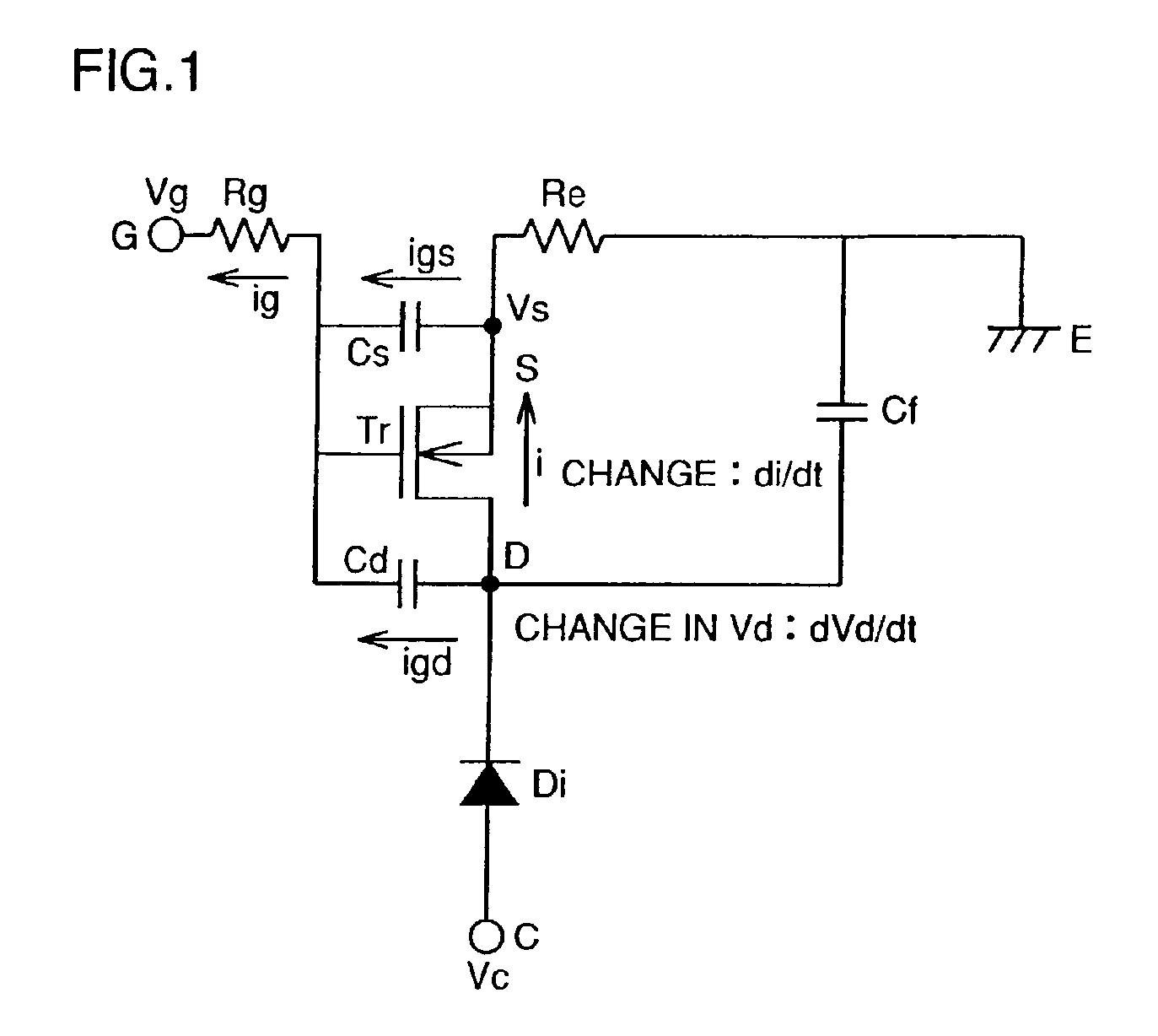
[0163]FIGS. 1 and 2 are a circuit diagram and a schematic cross sectional view showing the configuration of a semiconductor device according to Embodiment 1 of the present invention.

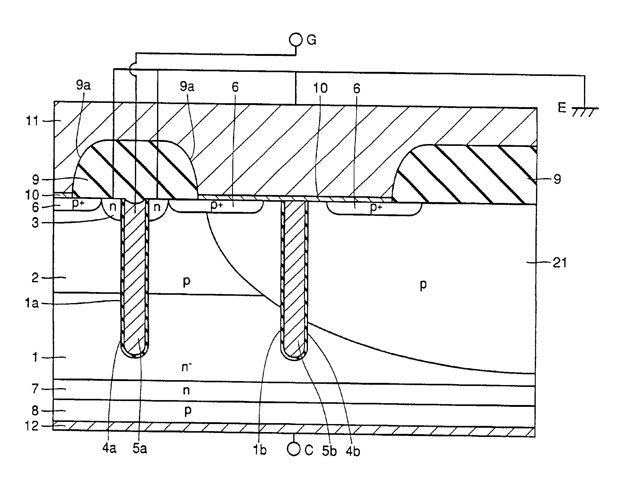
[0164]Referring primarily to FIG. 2, the semiconductor device of the present embodiment is a trench gate type IGBT formed in a semiconductor substrate having a thickness of, for example, 100 μm to 200 μm. An n− silicon substrate 1 has a concentration of, for example, approximately 1×1014 cm−3. A p-type body region 2 made of a p-type semiconductor, of which the concentration is, for example, approximately 1×1016 cm−3 to 1×1018 cm−3 and of which the depth from the first main surface is approximately 3 μm, is formed on the first main surface side of the above n− silicon substrate 1. An n-type emitter region 3 made of an n-type semiconductor, of which the concentration is, for example, 1×1019 cm−3, or higher, and of which the depth from the first main surface is approximately 0.5 μm, is f...

embodiment 2

[0202](Embodiment 2)

[0203]FIG. 8 is a cross sectional view schematically showing the configuration of a semiconductor device according to Embodiment 2 of the present invention. In reference to FIG. 8, the semiconductor device of the present embodiment is a plane gate-type IGBT that is formed in a semiconductor substrate of which the thickness is, for example, approximately 100 μm to 200 μm. A p-type body region 2 made of a p-type semiconductor is selectively formed on the first main surface side of an n− silicon substrate 1 having a concentration of, for example, approximately 1×1014 cm−3. p-type body region 2 has a concentration of, for example, approximately 1×1016 cm−3 to 1×1018 cm−3 and has a depth of approximately 3 μm from the first main surface. An n-type emitter region 3 made of an n-type semiconductor having a concentration of, for example, 1×1019 cm−3, or greater, of which the depth from the first main surface is approximately 0.5 μm is formed in the first main surface wit...

embodiment 3

[0214](Embodiment 3)

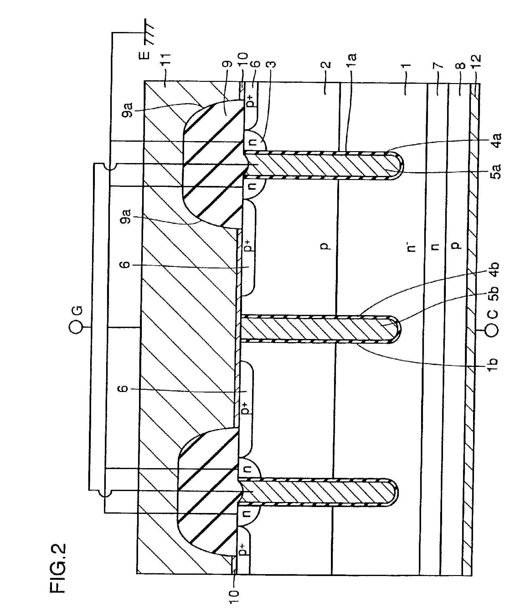
[0215]FIG. 9 is a cross sectional view schematically showing the configuration of a semiconductor device according to Embodiment 3 of the present invention. In reference to FIG. 9, the configuration of the present embodiment differs from the configuration of Embodiment 1 in the relationship between trench 1a for a gate and the depth of trench 1b for an emitter. In the present embodiment, depth D2 where trench 1b for an emitter extends within the n− silicon substrate is set at a value greater than depth D1 where trench 1a for a gate extends within the n− silicon substrate. Thereby, a stabilizing plate capacitor Cf formed between stabilizing plate 5b and n− silicon substrate 1 has a capacitance greater than that of a capacitor Cd on the gate side formed between gate electrode 5a and n− silicon substrate 1.

[0216]Here, each depth D3 or D4 of trench 1a for gate or of trench 1b for an emitter from the first main surface is within a range of, for example, from 3 μm to 1...


PUM


Abstract

A semiconductor device of the present invention has an insulating gate type field effect transistor portion having an n-type emitter region (3) and an n− silicon substrate (1), which are opposed to each other sandwiching a p-type body region (2), as well as a gate electrode (5a) which is opposed to p-type body region (2) sandwiching a gate insulating film (4a), and also has a stabilizing plate (5b). This stabilizing plate (5b) is made of a conductor or a semiconductor, is opposed to n− silicon substrate (1) sandwiching an insulating film (4, 4b) for a plate, and forms together with n− silicon substrate (1), a capacitor. This stabilizing plate capacitor formed between stabilizing plate (5b) and n− silicon substrate (1) has a capacitance greater than that of the gate-drain capacitor formed between gate electrode (5a) and n− silicon substrate (1).

Description

TECHNICAL FIELD[0001]The present invention relates to a semiconductor device and to a high voltage withstanding semiconductor device in which suppression of short circuiting current, reduction in gate capacitance and suppression of oscillation at the time of short circuiting can be achieved at the same time.BACKGROUND ART[0002]In the field of a high voltage withstanding semiconductor device that controls a voltage exceeding several hundred volts, element characteristics wherein heat emission, that is to say, loss is suppressed are required because the current handled is great. In addition, as for a driving system of a gate that controls this voltage and current, a voltage drive element of which the driving circuit is small so that the loss therein is small is desirable.[0003]In recent years, because of the above described reasons, an insulated gate bipolar transistor, that is to say, an IGBT, has come into wide use as an element wherein a voltage drive is possible and loss is small ...

Claims


Application Information

Patent Timeline
Patent Type & Authority Patents(United States)
IPC IPC(8): H01L29/06H01L29/66H01L29/02H01L29/739H01L29/417H01L29/40H01L29/45H01L31/0328
CPCH01L29/402H01L29/407H01L29/7395H01L29/7397H01L29/41741H01L29/456H01L21/18
Inventor NAKAMURA, KATSUMIKUSUNOKI, SHIGERUNAKAMURA, HIDEKI
Owner MITSUBISHI ELECTRIC CORP
Why Eureka
Try Eureka