Optically pumped, surface-emitting semiconductor laser device and method for the manufacture thereof

a laser device and surface-emitting technology, applied in the direction of lasers, semiconductor laser arrangements, semiconductor lasers, etc., can solve the problems of reducing the overall reducing the efficiency of the system, and few quantum wells can be excited by pump radiation, etc., to achieve simple manufacturing method, high output power, and simple adjustment of pump source and surface-emitting layer structur

Inactive Publication Date: 2005-10-11
OSRAM OLED
View PDF19 Cites 39 Cited by
  • Summary
  • Abstract
  • Description
  • Claims
  • Application Information

AI Technical Summary

Benefits of technology

[0009]According to the invention, the radiation-generating quantum well structure and the edge-emitting semiconductor structure are epitaxially grown on a common substrate given an optically pumped surface-emitting semiconductor laser device of the species initially cited. The layer thicknesses of the individual semiconductor layers can be very exactly set in the epitaxy, so that a high positioning precision of the edge-emitting semiconductor structure relative to the radiation-generating quantum well structure is advantageously achieved.
[0050]In order to prevent disturbing transverse modes (modes parallel to the substrate—whispering modes), absorber layers are arranged in the edge region and / or in etching structures of the surface-emitting semiconductor laser layer sequence.

Problems solved by technology

A particular problem given this known device is comprise therein that the pump laser must be exactly positioned relative to the surface-emitting semiconductor layer structure and, additionally, requires an optical means for beam focusing in order to image the pump radiation exactly into the desired region of the surface-emitting semiconductor layer structure.
These measures involve considerable technological outlay.
In addition to the losses at the optics, moreover, coupling losses also occur that reduce the overall efficiency of the system.
Another problem is comprised therein that only a few quantum wells can be excited by pump radiation due to the pumping from the front.

Method used


Image

  • Optically pumped, surface-emitting semiconductor laser device and method for the manufacture thereof
  • Optically pumped, surface-emitting semiconductor laser device and method for the manufacture thereof
  • Optically pumped, surface-emitting semiconductor laser device and method for the manufacture thereof

Examples


Embodiment Construction

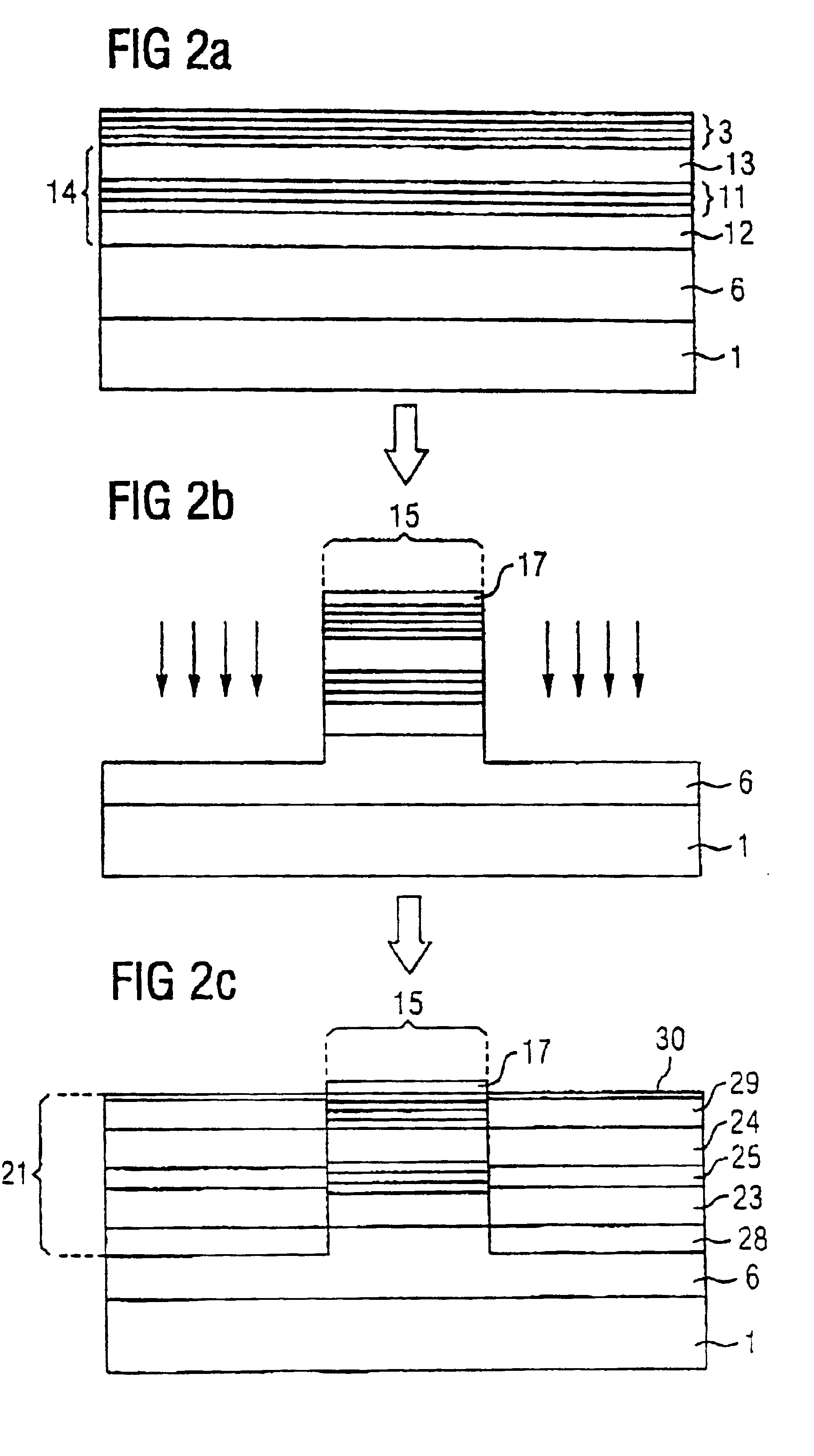
[0069]Identical elements or elements having the same effect are provided with the same reference characters in the Figures.

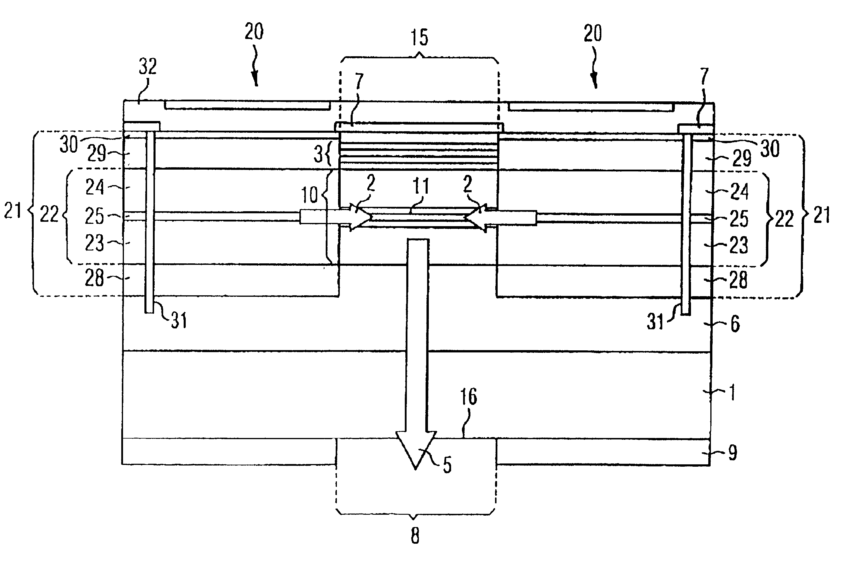
[0070]The exemplary embodiment of FIG. 1 is, for example, an optically pumped surface-emitting semiconductor laser chip having a laser emission at 1030 nm. Therein, a buffer layer 6 is applied on a substrate 1. The substrate 1 is composed, for example, of GaAs and the buffer layer 6 is composed of undoped GaAs.

[0071]A surface-emitting semiconductor laser structure 10 having a quantum well structure 11 is applied on the buffer layer 6 centrally over the substrate, this representing the surface-emitting laser region 15. The semiconductor laser structure 10 is composed of a first confinement layer 12 located directly on the buffer layer 6, of a quantum well structure 11 arranged on the confinement layer 12 and of a second confinement layer 13 applied on the quantum well structure 11.

[0072]The confinement layers 12 and 13 are composed, for example, of undoped GaAs, ...


PUM


Abstract

The invention is directed to an optically pumped surface-emitting semiconductor laser device having at least one radiation-generating quantum well structure and at least one pump radiation source for optically pumping the quantum well structure, whereby the pump radiation source comprises an edge-emitting semiconductor structure. The radiation-generating quantum well structure and the edge-emitting semiconductor structure are epitaxially grown on a common substrate. A very efficient and uniform optical pumping of the radiation-generating quantum well structure is advantageously possible with this monolithically produced semiconductor laser device. Methods for manufacturing inventive semiconductor laser devices are also specified.

Description

BACKGROUND OF THE INVENTION[0001]1. Field of the Invention[0002]The invention is directed to an optically pumped surface-emitting semiconductor laser device having at least one radiation-generating quantum well structure and at least one pump radiation source for optically pumping the quantum well structure, whereby the pump radiation source comprises an edge-emitting semiconductor structure.[0003]2. Description of the Related Art[0004]A semiconductor laser device of the species initially described is disclosed by U.S. Pat. No. 5,991,318. An optically pumped vertical resonator semiconductor laser having a monolithic surface-emitting semiconductor layer structure is disclosed therein. Given this known device, the optical pump radiation, whose wavelength is shorter than that of the generated laser emission, is supplied by an edge-emitting semiconductor laser diode. The edge-emitting semiconductor laser diode is externally arranged such that the pump radiation is beamed obliquely in fr...

Claims


Application Information

Patent Timeline
Patent Type & Authority Patents(United States)
IPC IPC(8): H01S5/00H01S5/183H01S5/04H01S5/40H01S5/026H01S5/10H01S5/14H01S5/34
CPCB82Y20/00H01S5/026H01S5/041H01S5/141H01S5/183H01S5/18305H01S3/1062H01S3/109H01S5/1071H01S5/1075H01S5/16H01S5/2022H01S5/3432H01S5/4056H01S2301/166H01S5/1017H01S5/1082H01S5/1835H01S5/2214H01S5/34313H01S5/4031
Inventor ALBRECHT, TONYLINDER, NORBERTLUFT, JOHANN
Owner OSRAM OLED
Why Eureka
Try Eureka