Method for defining a minimum pitch in an integrated circuit beyond photolithographic resolution

a technology of photolithographic resolution and integrated circuit, which is applied in the direction of basic electric elements, electrical apparatus, semiconductor devices, etc., can solve the problems of insufficient adhesion of structures formed using this method, the fundamental limitation of photolithographic resolution of light sources used, and the drawback of art, etc., to achieve the effect of minimising the pitch of polysilicon in the memory array region

Active Publication Date: 2005-10-18
MACRONIX INT CO LTD
View PDF4 Cites 247 Cited by
  • Summary
  • Abstract
  • Description
  • Claims
  • Application Information

AI Technical Summary

Benefits of technology

[0006]One object of the present invention is to provide a method for defining a minimum pitch in an integrated circuit beyond photolithographic resolution, so as to resolve difficulties as photolithographic resolution being restricted by the wavelength of light source used.
[0009]Furthermore, in this method, the minimum polysilicon pitch in the memory array region on photomask is enlarged and the initial minimum polysilicon pitch in the periphery region on photomask can be reduced. It helps overcoming the difficulty of a significant difference in polysilicon pitch between the memory array region and periphery region in conventional approaches.

Problems solved by technology

However, photolithographic resolution is fundamentally restricted by the wavelength of light sources used.
However, structures formed using this method are prone to drawbacks as having relatively insufficient adherence.
However, this art has a drawback as the hard buffer layer being not so easily deposited.

Method used


Image

  • Method for defining a minimum pitch in an integrated circuit beyond photolithographic resolution
  • Method for defining a minimum pitch in an integrated circuit beyond photolithographic resolution
  • Method for defining a minimum pitch in an integrated circuit beyond photolithographic resolution

Examples


first embodiment

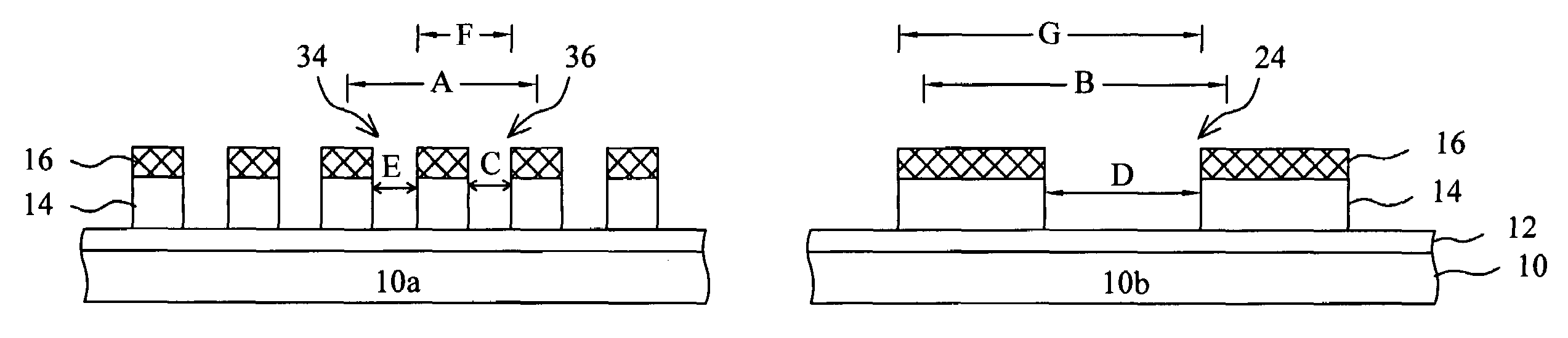
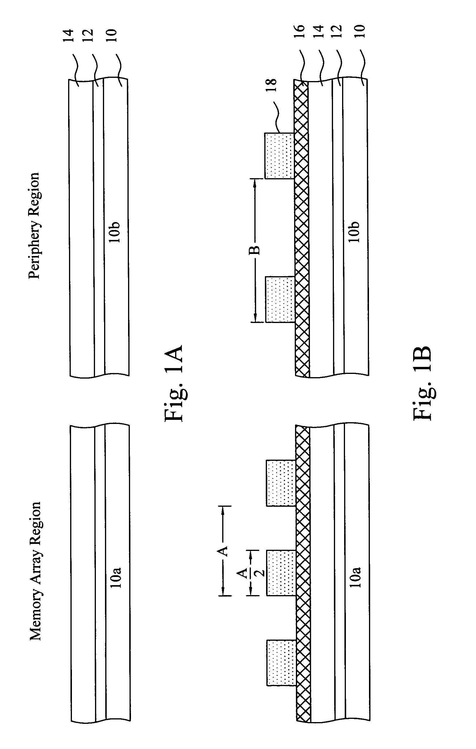
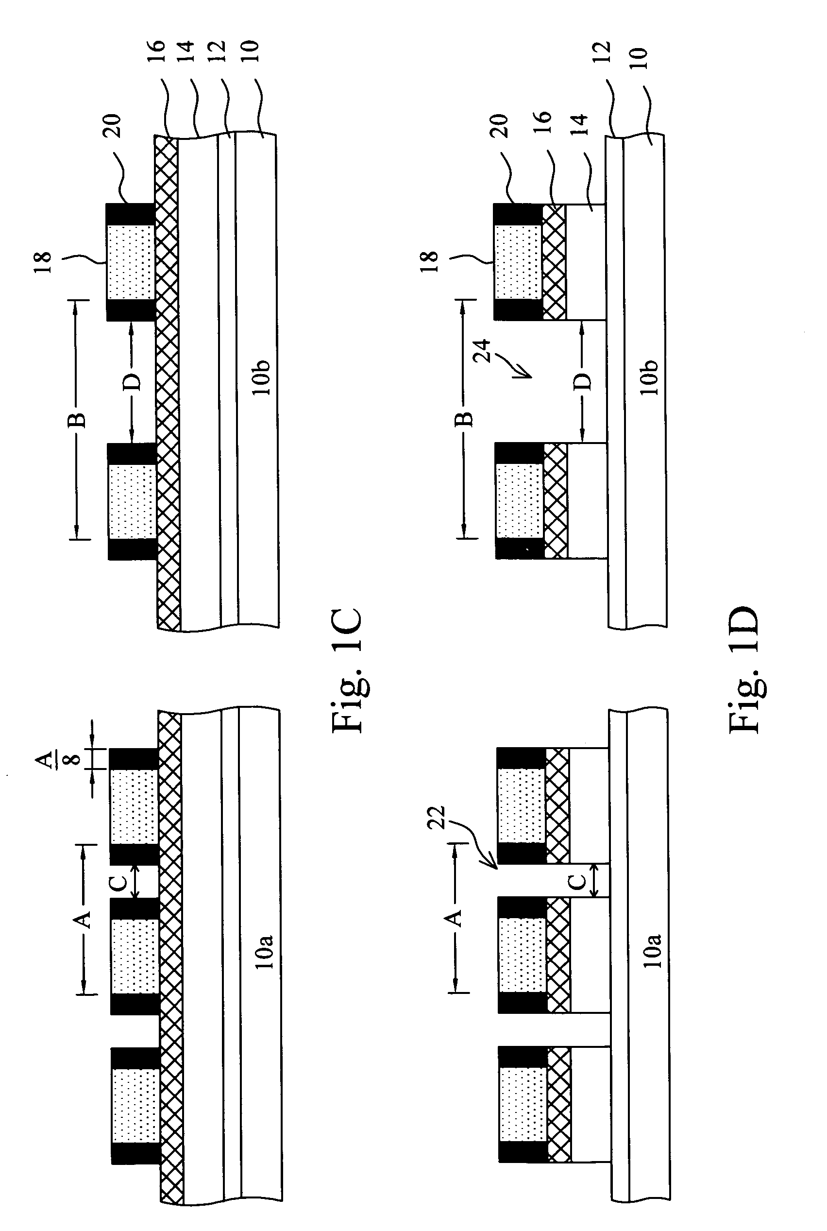
[0013]FIGS. 1A–1I show a first embodiment according to the present invention. Referring to FIG. 1A, an oxide 12 and a polysilicon 14 are deposited on a substrate 10 on which a memory array region 10a and a periphery region 10b are defined. The polysilicon 14 is the target layer that will be formed with pitches beyond photolithographic resolution in the following process. An anti-reflection coating (ARC) 16 and a photoresist 18 are applied on the polysilicon 14, and a photoresist pattern 18 is defined to the photoresist 18 after exposure and development. The minimum pitch in the memory array region 10a is A and the minimum pitch in the periphery region 10b is B. Pitch is defined as the sum of a line width and a line space, and preferably, both the line width and the space in the memory array region are A / 2, as shown in FIG. 1B.

[0014]Referring to FIG. 1C, polymer spacers 20 are formed on each sidewall of the photoresist pattern 18. This polymer 20 is deposited only on the sidewalls of...

second embodiment

[0016]FIGS. 2A–2I show another embodiment according to the present invention. An oxide 52 and a polysilicon 54 are deposited onto a substrate 50, on which a memory array region 50a and a periphery region 50b are to be defined, and the polysilicon 54 in the memory array region 50a is the target layer to have the pitch beyond photolithographic resolution. Referring to FIG. 2B, a buffer layer 56, for example, oxide or silicon nitride of sufficiently high etch selectivity with respect to polysilicon 54 is further deposited. An ARC 58 and a photoresist 60 are applied thereon, and a photoresist pattern 60 is defined by exposure and development processes. The minimum pitch in the memory array region 50a is referred to as A, and the minimum pitch in the periphery region 50b is referred to as B. Preferably, a line width and a line space of the pitch A are both A / 2.

[0017]Referring to FIG. 2C, polymer spacers 62 are formed on the sidewalls of the photoresist pattern 60. Preferably, the width o...


PUM


Abstract

A method for defining a minimum pitch in an integrated circuit beyond photolithographic resolution controls the defined pitches of the target layer by use of polymer spacer, photo-insensitive polymer plug and polymer mask during the process, so as to achieve the minimum pitch of the target layer beyond photolithographic resolution. Applied to memory manufacture, this method is capable of simultaneously overcoming the process difficulty of significant difference between polysilicon pitches in memory array region and periphery region.

Description

FIELD OF THE INVENTION[0001]The present invention relates generally to the manufacture of an integrated circuit (IC) and more particularly, to a method for defining a minimum pitch in an integrated circuit beyond photolithographic resolution.BACKGROUND OF THE INVENTION[0002]Generally, the growth of integrated circuit industry depends on the continuous advancement in photolithographic technologies in integrated circuit manufacture. Propelled by advancement of photolithographic technologies, integrated circuits have repeatedly achieving the targets of higher density and smaller size. Hence, critical dimension (CD), including both minimum line width and space, of integrated circuits also has become finer and finer, indicating that higher resolutions are required. However, photolithographic resolution is fundamentally restricted by the wavelength of light sources used. To overcome such restriction, numerous methods provided by prior arts are available.[0003]Referring to U.S. Pat. No. 5,...

Claims


Application Information

Patent Timeline
Patent Type & Authority Patents(United States)
IPC IPC(8): H01L21/70H01L21/8242H01L21/033H01L21/3213
CPCH01L21/0337H01L21/0338H01L21/32139H01L27/10894Y10S438/947H10B12/09
Inventor CHUNG, HENRY
Owner MACRONIX INT CO LTD
Why Eureka
Try Eureka