Transfer molding of integrated circuit packages

Inactive Publication Date: 2005-10-18
GLOBALFOUNDRIES US INC
View PDF11 Cites 9 Cited by
  • Summary
  • Abstract
  • Description
  • Claims
  • Application Information

AI Technical Summary

Benefits of technology

[0012]It is an object of the present invention to provide improved techniques resulting in a more uniform and controlled flow of encapsulant for more

Problems solved by technology

Since the substrate and the integrated circuit chip have different coefficients of thermal expansion, they expand and contract at different rates, possibly causing the solder ball connections to weaken or even crack as a result of fatigue.
It may be desirable in some cases to further alter the cured properties of the encapsulant, however, the requirement that the encapsulant have low viscosity in the uncured state severely restricts the formulation options.
For example, the addition of more ceramic filler would lower the resulting coefficient of thermal expansion, but increase the uncured viscosity.
This approach essentially eliminates the small gap typical of a conventional integrated circuit chip to substrate interc

Method used


Image

  • Transfer molding of integrated circuit packages
  • Transfer molding of integrated circuit packages
  • Transfer molding of integrated circuit packages

Examples


Embodiment Construction

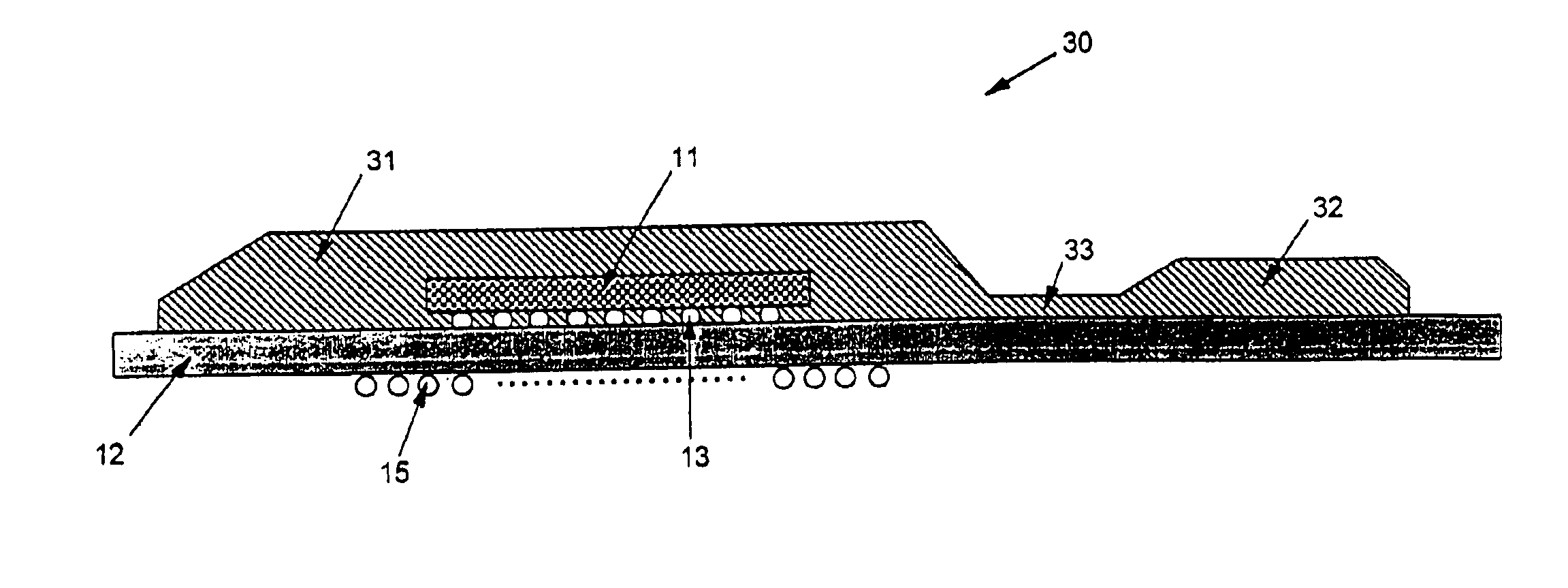
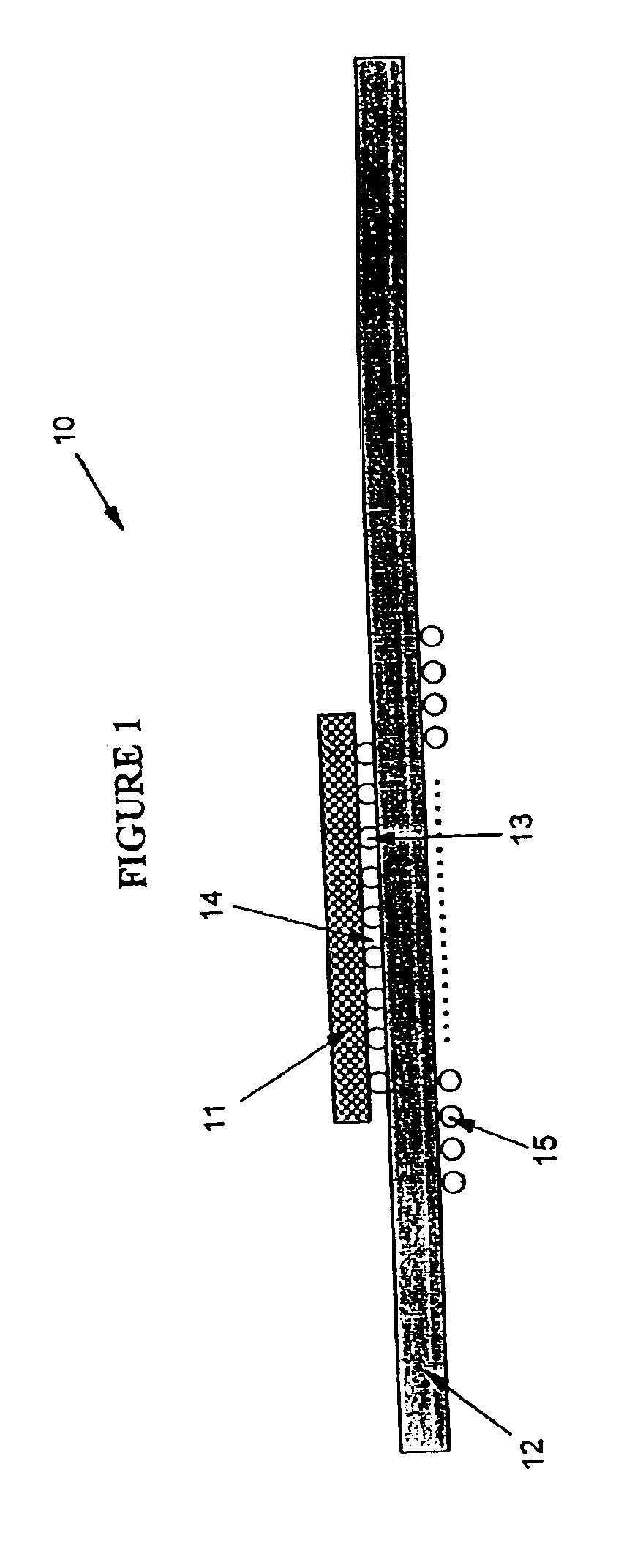
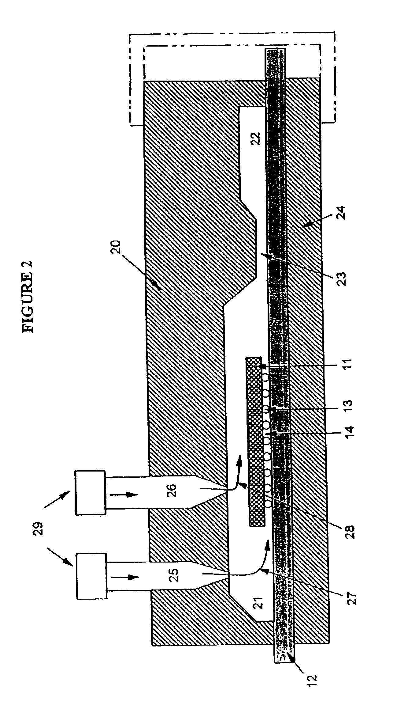
[0025]Proper encapsulation of a flip chip integrated circuit module with currently available transfer molding or over-molding encapsulating processes, raises a number of problems and thus is a generalized concern. It is, of course, desirable to encapsulate the flip chip module on a substrate to strengthen and reinforce the physical connections between the flip chip module and the substrate but at the same time, to ensure all air is removed to minimize humidity absorption and points of stress caused from any entrapped air. Underfill is desirable to reduce the stress on the solder joints resulting from the normal cycling of the module during operation and the different temperature coefficients of the module and the substrate to thereby prolong the fatigue life of the package before failure occurs. Any sharp corners of a mold could result in air being entrapped within the encapsulation and this is undesirable. Present processes tend to also cause restrictions which impact the possible ...


PUM

PropertyMeasurementUnit
Heightaaaaaaaaaa

Abstract

A method, mold and apparatus for encapsulating and underfilling an integrated circuit chip assembly. The mold has a first portion and a second portion with the first portion having first and second cavities and at least one channel interconnecting said first and second cavities. The first cavity is adapted to enclose said integrated circuit chip on said substrate. A clamping force is applied to the first and second portions of the mold to clamp the substrate between them with the integrated circuit chip located in the first cavity. Vents exhaust air from the first cavity. Encapsulant is injected into the first cavity of the first portion at a location in the first portion remote from the point of connection of the channel such that encapsulant flows around and underneath the integrated circuit chip and through the channel into the second cavity to thereby underfill and encapsulate the integrated circuit assembly.

Description

CROSS-REFERENCE TO RELATED APPLICATION[0001]This application is a divisional of application Ser. No. 10 / 167,635, filed Jun. 12, 2002, now U.S. Pat. No. 6,656,773.FIELD OF THE INVENTION[0002]This invention relates to an improved method of the use of transfer molding for encapsulating and underfilling integrated circuit chips attached to substrates to result in integrated circuit packages. It also relates to the mold and apparatus used in the improved method and the resultant integrated circuit assemblies.BACKGROUND OF THE INVENTION[0003]An integrated circuit chip assembly generally comprises an integrated circuit chip attached to a substrate, typically a chip carrier or a circuit board. The most commonly used integrated circuit chip is composed primarily of silicon having a coefficient of thermal expansion of about 2 to 4 ppm / ° C. The chip carrier or circuit board is typically composed of either a ceramic material having a coefficient of thermal expansion of about 6 ppm / ° C., or an o...

Claims


Application Information

Patent Timeline
IPC IPC(8): H01L21/56H01L23/31H01L23/34
CPCH01L21/563H01L21/565H01L23/3128H01L2224/16H01L2224/83104H01L2924/00014H01L2924/15311H01L2924/1815H01L2224/0401
Inventor BOYAUD, MARIE-FRANCEDUFORT, CATHERINEPAQUET, MARIE-CLAUDETETREAULT, REAL
Owner GLOBALFOUNDRIES US INC
Why Eureka
Try Eureka