Method of forming a magnetic tunneling junction (MTJ) MRAM device and a tunneling magnetoresistive (TMR) read head

Active Publication Date: 2005-11-01
APPLIED SPINTRONICS +1
View PDF8 Cites 55 Cited by
  • Summary
  • Abstract
  • Description
  • Claims
  • Application Information

AI Technical Summary

Benefits of technology

[0017]A fourth object of the present invention is to provide an MTJ MRAM element having well controlled free layer magnetization, well controlled magnetization of the pinned layer as evidenced by a large exchange field and thermal stability and a tunneling barrier layer with physical integrity.
[0018]The objects of the present

Problems solved by technology

Whether it is used as an MRAM or as a TMR read head, fabrication of a high quality MTJ device presents considerable difficulties due to the necessity of forming layers of extreme thinness.
This is itself a problem, since the layers are exceptionally thin.
Second, the resistance of the tunneling barrier layer is

Method used


Image

  • Method of forming a magnetic tunneling junction (MTJ) MRAM device and a tunneling magnetoresistive (TMR) read head
  • Method of forming a magnetic tunneling junction (MTJ) MRAM device and a tunneling magnetoresistive (TMR) read head
  • Method of forming a magnetic tunneling junction (MTJ) MRAM device and a tunneling magnetoresistive (TMR) read head

Examples


first embodiment

[0036]The present invention, in a first preferred embodiment, is a method of forming an MTJ MRAM by the use of a novel NiCr seed layer formed on a sputter-etched Ta layer so that the subsequently formed tunneling junction layer is ultra-thin and smooth and has a high breakdown voltage. In a second preferred embodiment the present invention is a method of forming a TMR read head having a high GMR ratio, low junction resistance and high tunneling layer breakdown voltage, using the novel NiCr seed layer formed on a sputter-etched Ta layer.

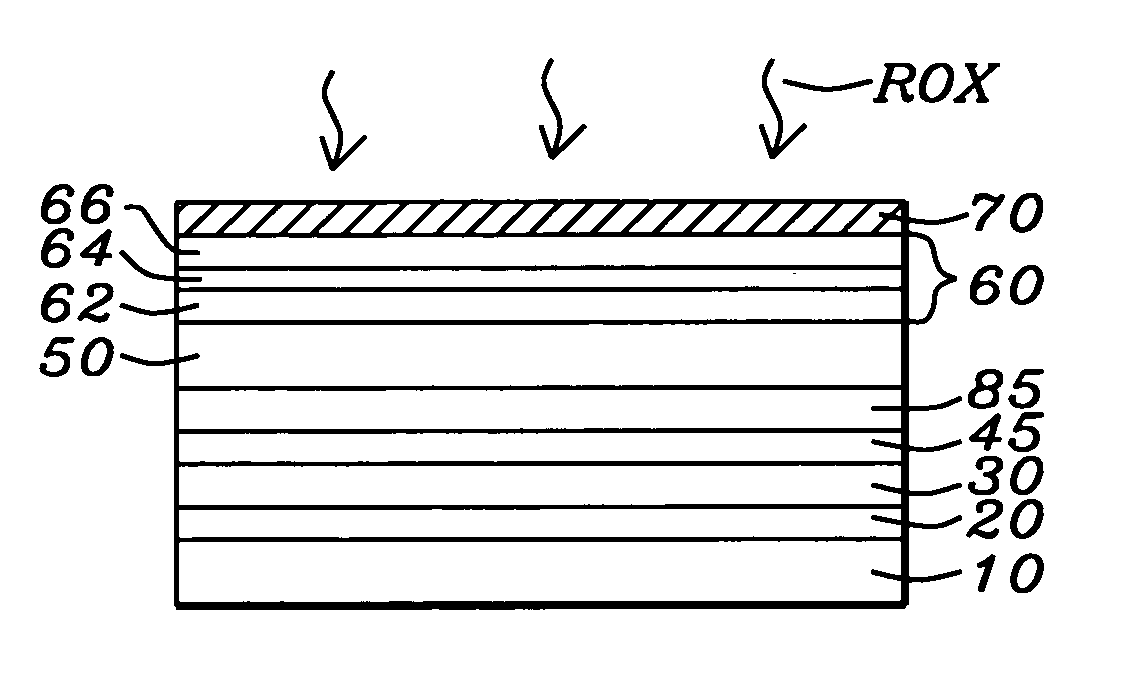
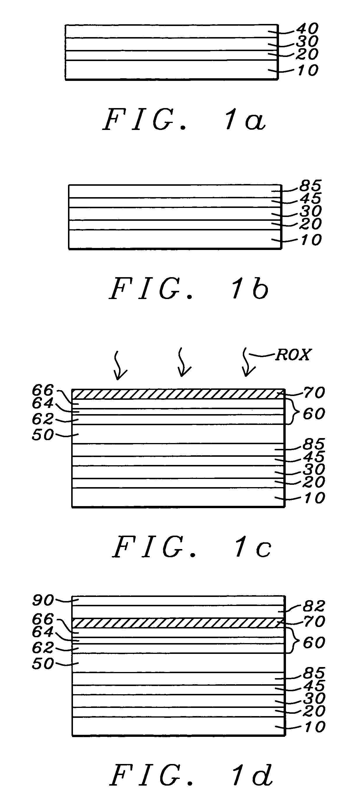
[0037]Referring now to FIG. 1a, there is seen in a schematic cross section an initial stage of a preferred embodiment of the invention, the formation of a single MRAM element, which can be a part of an array of such elements. It is to be understood that in the embodiments to be disclosed in what follows, all layer depositions take place in an ultra- high vacuum system suitable for depositing thin layers by sputtering. In these embodiments the system w...

second embodiment

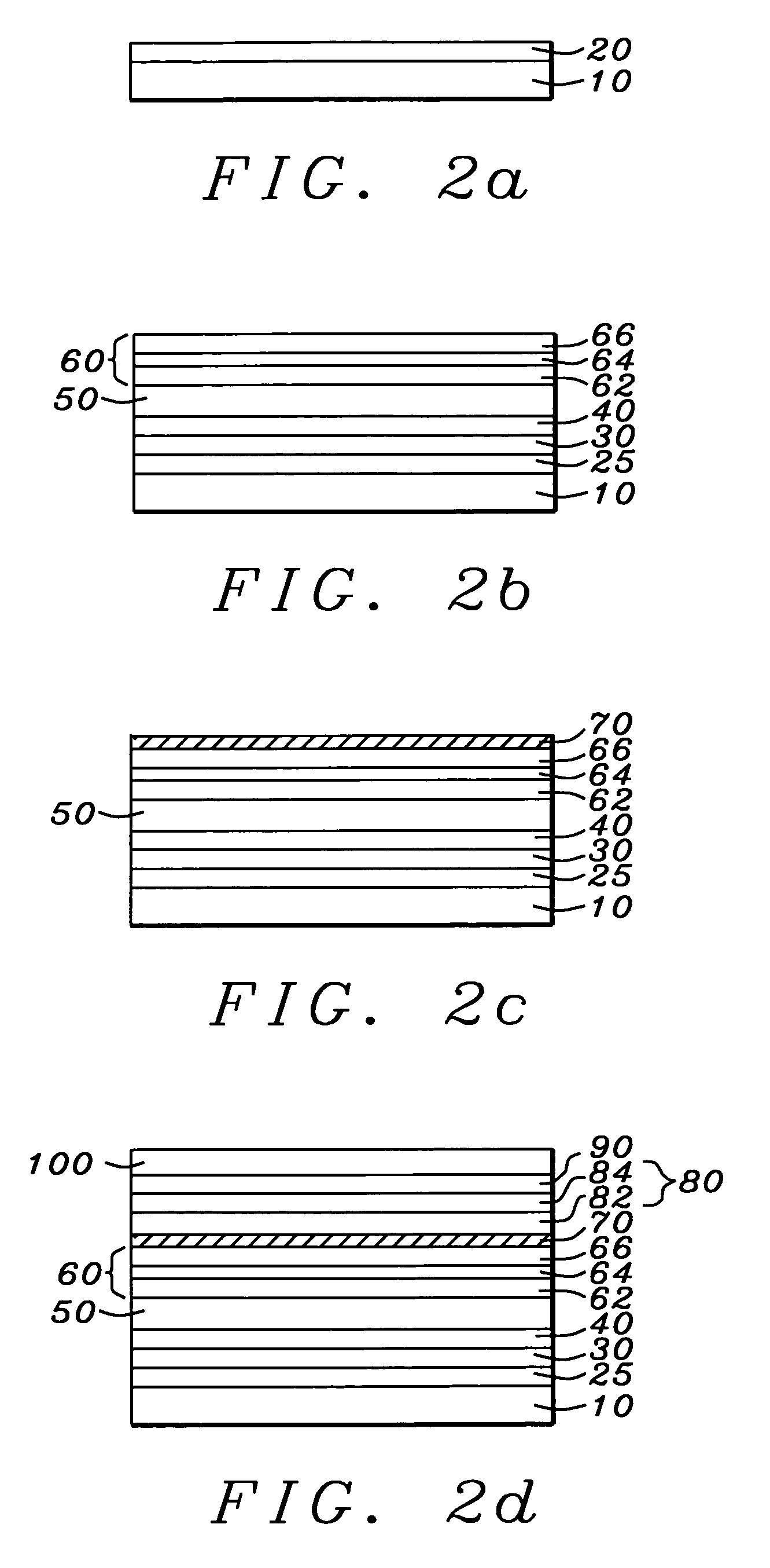
[0043]Referring now to FIG. 2a, there is seen a schematic cross-sectional view of the initial steps of a second embodiment of the present invention, which is the formation of a TMR read sensor. As in the MRAM formation described above, the TMR read sensor is also formed as a series of layers in the sputtering chamber of an ultra-high vacuum sputtering system. It is to be noted, although it is known to those skilled in the art, that the tunneling magnetic junction configuration, when used to form an MRAM element as in the first embodiment, is formed between a word line and a bit line, insulated from the former and contacting the latter, whereas the tunneling magnetic junction configuration, when used to form a magnetoresistive read sensor, ie a TMR sensor, is formed between upper and lower magnetic shields, contacting them both since they serve as conducting leads.

[0044]Referring again to FIG. 2a, there is first seen a substrate (10), which in this embodiment could be a lower shield / ...


PUM

PropertyMeasurementUnit
Fractionaaaaaaaaaa
Pressureaaaaaaaaaa
Poweraaaaaaaaaa

Abstract

An MTJ (magnetic tunneling junction) device particularly suitable for use as an MRAM (magnetic random access memory) or a tunneling magnetoresistive (TMR) read sensor, is formed on a seed layer which allows the tunneling barrier layer to be ultra-thin, smooth, and to have a high breakdown voltage. The seed layer is a layer of NiCr which is formed on a sputter-etched layer of Ta. The tunneling barrier layer for the MRAM is formed from a thin layer of Al which is radically oxidized (ROX), in-situ, to form the layer with characteristics described above. The tunneling barrier layer for the read sensor formed from a thin layer of Al or a HfAl bilayer which is naturally oxidized (NOX), in situ, to form the barrier layer. The resulting device has generally improved performance characteristics in terms of GMR ratio and junction resistance.

Description

RELATED PATENT APPLICATION[0001]This application is related to Ser. No. 10 / 371,841 filing date, Feb. 20, 2003, now issued as U.S. Pat. No. 6,703,645; Ser. No. 10 / 820,391, filing date Apr. 8, 2004 and Ser. No. 10 / 768,917, filing date Jan. 30, 2004, assigned to the same assignee as the current invention.BACKGROUND OF THE INVENTION[0002]1. Field of the Invention[0003]This invention relates generally to magnetic tunneling junction (MTJ) devices such as MRAMs and read-heads and more particularly to the use of a novel seed layer that allows the formation of a junction layer of superior physical properties.[0004]2. Description of the Related Art[0005]The magnetic tunneling junction device (MTJ device) is essentially a variable resistor in which the relative orientation of magnetic fields in an upper and lower very thin dielectric layer (the tunneling barrier layer) formed between those electrodes. As electrons pass through the upper electrode they are spin polarized by its magnetization di...

Claims


Application Information

Patent Timeline
IPC IPC(8): G11C11/15G11C11/16G11C11/02H01L21/70H01L21/8246H01L43/08G11B5/39H01F10/30H01F10/32H01F41/18H01F41/30H01L27/105H01L43/10H01L43/12
CPCB82Y25/00B82Y40/00G11C11/16H01F10/30H01F10/3295H01F41/307H01L43/08H01L43/12H01F10/3272G11C11/161H10N50/01H10N50/10H10B61/00
Inventor HORNG, CHENG T.HONG, LIUBOTONG, RU-YINGCHEN, YU-HSIA
Owner APPLIED SPINTRONICS
Why Eureka
Try Eureka