Dual-counterdoped channel field effect transistor and method

a field effect transistor and counter-doping technology, applied in the field of dual-counter-doping channel field effect transistors and methods, can solve the problems of high level of doping, etc., and achieves the effect of reducing the concentration of dopant, reducing the switching speed of the fet, and reducing the mobility of the charge carrier

Inactive Publication Date: 2005-11-01
TEXAS INSTR INC
View PDF6 Cites 20 Cited by
  • Summary
  • Abstract
  • Description
  • Claims
  • Application Information

AI Technical Summary

Benefits of technology

[0004]Therefore, a need has arisen for an improved field effect transistor that addresses the disadvantages and deficiencies of the prior art.
[0005]A field effect transistor with a dual-counterdoped channel in accordance with the present invention is disclosed. The transistor features a channel comprising first and second doped regions. The second doped region underlies the first doped region. A source and drain are formed adjacent to the channel. In one embodiment of the present invention, the first doped region comprises an arsenic dopant, while the second doped region comprises a phosphorus dopant.
[0006]A technical advantage is that subsurface channel layer is formed in the central portion of the channel that has greater charge-carrier mobility than conventional surface channels, thus allowing a lower dopant concentration to be used in the subsurface channel layer without negatively affecting transistor performance. Another technical advantage is that the lower subsurface channel doping allows lower source / drain pocket doping, thus reducing the capacitance and response time of the transistor. Yet another technical advantage is that the channel length of the transistor may be decreased without increasing the capacitance and response time of the transistor to unacceptable levels. Yet another technical advantage is that chip size may be reduced, thereby increasing yield from a single wafer and decreasing chip cost.

Problems solved by technology

However, to achieve this result, a high level of doping is necessary in the pockets around the source and drain regions to counteract the effect of the counterdoping in the channel.
The high level of doping results in high source and drain capacitances, thus decreasing the switching speed of the FET.

Method used


Image

  • Dual-counterdoped channel field effect transistor and method
  • Dual-counterdoped channel field effect transistor and method
  • Dual-counterdoped channel field effect transistor and method

Examples


Embodiment Construction

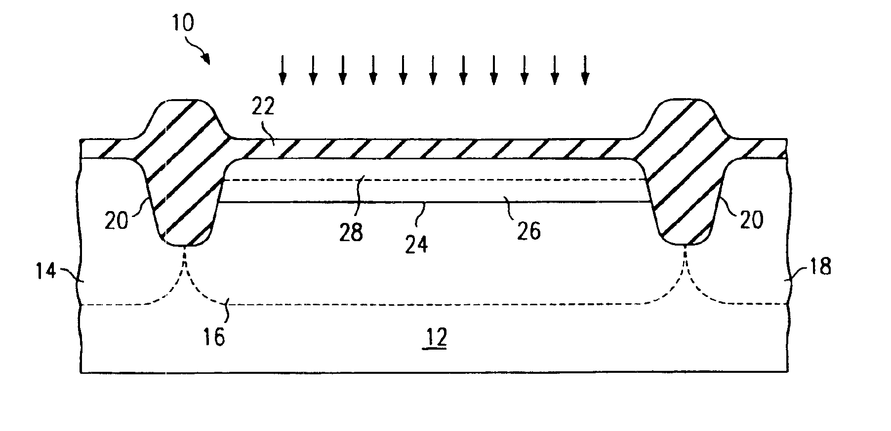
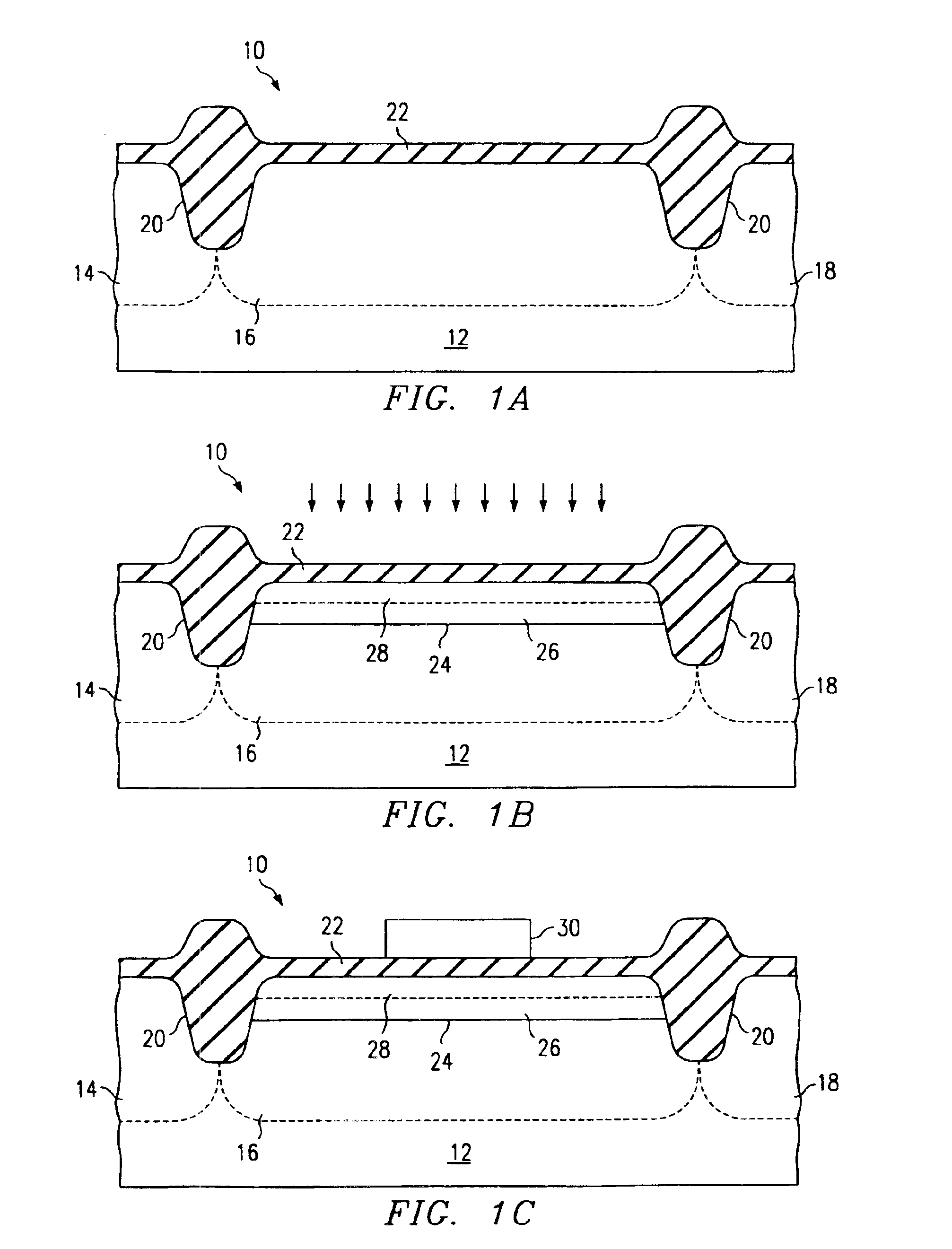
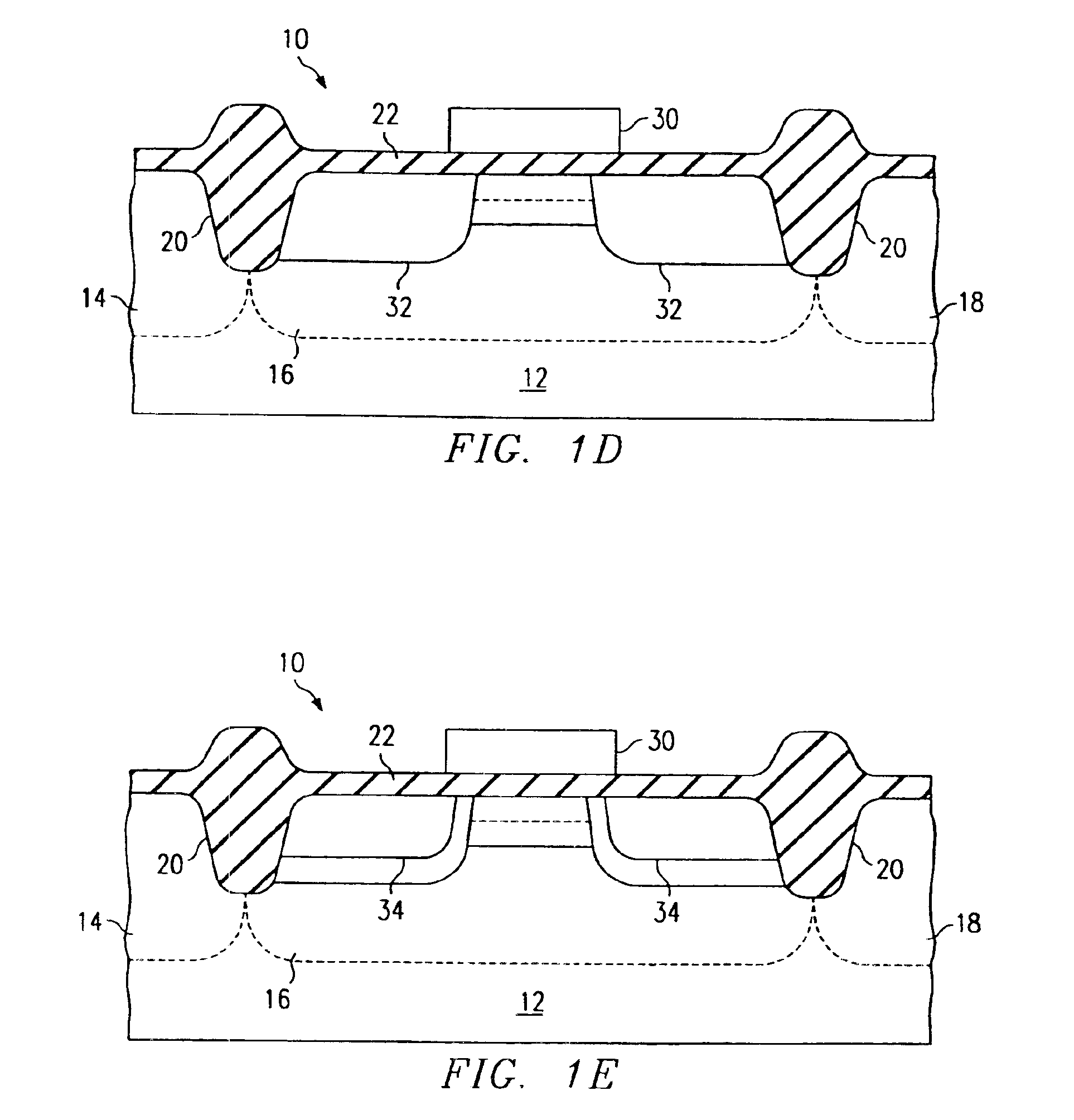
[0009]FIGS. 1A through 1E illustrate a method for forming a semiconductor device having a dual-counterdoped channel field effect transistor in accordance with the present invention.

[0010]Referring to FIG. 1A, a cross section of a semiconductor device 10 during fabrication is shown. Semiconductor device 10 includes a substrate 12 which comprises silicon, silicon on insulator (SOI), or any other appropriate substrate for semiconductor fabrication. A plurality of doped wells 14, 16 and 18 are formed in substrate 12 using well-known techniques. For example, well 16 may be a p-type well, while wells 14 and 18 may be n-type wells. For purposes of illustration, well 16 will be assumed to be a p-type well in the following description. However, it will be understood that well 16 may be an n-type well, with the appropriate substitution of n-type dopants for p-type dopants (and vice versa) throughout the following description.

[0011]Wells 14, 16 and 18 are separated by isolation trenches 20, wh...


PUM


Abstract

A field effect transistor with a dual-counterdoped channel is disclosed. The transistor features a channel comprising a first doped region (28) and a second doped region (26) underlying the first doped region. A source and drain (32) are formed adjacent to the channel. In one embodiment of the present invention, the first doped region (28) is doped with arsenic, while the second doped region (26) is doped with phosphorus. The high charge-carrier mobility of the subsurface channel layer (28) allowing a lower channel dopant concentration to be used, which in turn allows lower source/drain pocket doping. This reduces the capacitance and response time of the transistor.

Description

[0001]This application is a division of Ser. No. 09 / 252,514, filed Feb. 18, 1999 now abandoned, which claims priority under 35 U.S.C. from provisional application Ser. No. 60 / 075,813, filed Feb. 24, 1998.TECHNICAL FIELD OF THE INVENTION[0002]This invention relates generally to semiconductor devices and more particularly to a dual-counterdoped channel field effect transistor and method.BACKGROUND OF THE INVENTION[0003]In the art of field effect transistor (FET) design, it is desirable to minimize the leakage (off-state) current while maximizing the drive (on-state) current of the FET. One known method for achieving this result is to surround the source and drain regions with pockets or halos of doping, while counterdoping the channel region. This practice minimizes the short-channel effects that negatively affect the performance of small-scale FETs. However, to achieve this result, a high level of doping is necessary in the pockets around the source and drain regions to counteract th...

Claims


Application Information

Patent Timeline
Patent Type & Authority Patents(United States)
IPC IPC(8): H01L21/265H01L21/02H01L29/10H01L29/02
CPCH01L21/2652H01L29/1033H01L21/2658
Inventor NANDAKUMAR, MAHALINGAMVASANTH, KARTHIKCHEN, IH-CHIN
Owner TEXAS INSTR INC
Why Eureka
Try Eureka